OOPS! You forgot to upload swfobject.js ! You must upload this file for your form to work.
IBM gives priority to the construction of multi-stage processors
![]()
|
xtreview is your : Video card - cpu - memory - Hard drive - power supply unit source |
|
|||
|
|
||||
 Recommended : Free unlimited image hosting with image editor
|
POSTER: computer news || IBM GIVES PRIORITY TO THE CONSTRUCTION OF MULTI-STAGE PROCESSORS |
DATE:2012-12-14 |
|
|
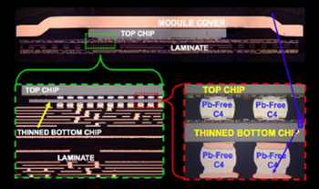
IBM begins to give priority to the so-called 3D-structures - multi-chip packages semiconductor circuits. Crystals can be packed in different ways: in a column, on the same horizon, with some crystals with conventional substrate using the interconnect wiring, and finally, using the through-plated channels (TSVs). The company is aware that the transition to a smaller scale process technology at this stage is more expensive . The company has repeatedly confirmed the readiness to work with TSVs-compounds. Basically, IBM became the first company to start to promote this idea, but in practice, perhaps the first of its wide use, Samsung started to release memory.  At the moment the conference International Electron Devices Meeting (IEDM) IBM representatives told about qualified 45nm server processor on SOI-substrate with integrated memory eDRAM, which is packaged in a single unit with two integrated SiGe BiCMOS-crystal transceivers. The capacity of the internal communication channels reached a value of 2 Tbit / s, which is more than a qualitative indicator promising work in this direction. But there are problems. The main one - is the connections through channels . As copper has a different coefficient of thermal expansion than the semiconductor crystal, thick copper channels during heating can literally blow up the chip . Therefore the design of the processor requires a lot of high-rise architectural tweaks. Related Products : | ||
|
|
||
|
xtreview is your : Video card - cpu - memory - Hard drive - power supply unit source |
|
|
|
|
||
|
Xtreview Support  N-Post:xxxx Xtreview Support        |
IBM GIVES PRIORITY TO THE CONSTRUCTION OF MULTI-STAGE PROCESSORS |
| Please Feel Free to write any Comment; Thanks  |
Debugging mechanism gives access to Intel processors over USB port (2017-01-13)
AutoPilot now on Tesla gives priority to information from sensors, not cameras (2016-09-12)
EVGA gives new case to all owners of video cards with hybrid cooling (2015-10-08)
LG gives all new customers Android-smartphone device G3 virtual reality (2015-02-10)
HTC gives Android-camera RE at half price (2014-11-26)
Google gives smart glass two gigabytes of memory (2014-06-25)
HP gives new printers direct printing from mobile devices (2014-03-18)
Google gives gifts starting price for smartphone Moto X is reduced to 399 dollars (2014-01-02)
IBM gives priority to the construction of multi-stage processors (2012-12-14)
Asus lowers the price of its tablet with Windows RT and gives customers a free dock station (2012-11-08)
Gigabyte gives overclockers an additional guarantee for Intel (2012-02-12)
HP gives printers the ability to print documents from Google cloud (2011-04-03)
![]()
To figure out your best laptops .Welcome to XTreview.com. Here u can find a complete computer hardware guide and laptop rating .More than 500 reviews of modern PC to understand the basic architecture


7600gt review
7600gt is the middle card range.
We already benchmarked this video card and found that ...

 geforce 8800gtx and 8800gts
  Xtreview software download Section
  AMD TURION 64 X2 REVIEW
  INTEL PENTIUM D 920 , INTEL PENTIUM D 930
  6800XT REVIEW
  computer hardware REVIEW
  INTEL CONROE CORE DUO 2 REVIEW VS AMD AM2
  INTEL PENTIUM D 805 INTEL D805
  Free desktop wallpaper
  online fighting game
  Xtreview price comparison center
 Lastest 15 Reviews


Rss Feeds
Last News
- The new version of GPU-Z finally kills the belief in the miracle of Vega transformation
- The motherboard manufacturer confirms the characteristics of the processors Coffee Lake
- We are looking for copper coolers on NVIDIA Volta computing accelerators
- Unofficially about Intels plans to release 300-series chipset
- The Japanese representation of AMD offered monetary compensation to the first buyers of Ryzen Threadripper
- This year will not be released more than 45 million motherboards
- TSMC denies the presentation of charges from the antimonopoly authorities
- Radeon RX Vega 64 at frequencies 1802-1000 MHz updated the record GPUPI 1B
- AMD itself would like to believe that mobile processors Ryzen have already been released
- AMD Vega 20 will find application in accelerating computations
- Pre-orders for new iPhone start next week
- Radeon RX Vega 57, 58 and 59: the wonders of transformation
- ASML starts commercial delivery of EUV-scanners
- The older Skylake processors with a free multiplier are removed from production
- Meizu will release Android-smartphone based on Helio P40
- AMD Bristol Ridge processors are also available in American retail
- The fate of Toshiba Memory can be solved to the next environment
- duo GeForce GTX 1080 Ti in GPUPI 1B at frequencies of 2480-10320 MHz
- New Kentsfield overclocking record up to 5204 MHz
- Lenovo released Android-smartphone K8

HALO 3 HALO 3 - Final Fight!

PREY Prey is something you don t often see anymore: a totally unigue shooter experience.

computer news computer parts review Old Forum Downloads New Forum Login Join Articles terms Hardware blog Sitemap Get Freebies


