OOPS! You forgot to upload swfobject.js ! You must upload this file for your form to work.
A little more detail about NVIDIA NVLink memory and 3D-Pascal
![]()
|
xtreview is your : Video card - cpu - memory - Hard drive - power supply unit source |
|
|||
|
|
||||
 Recommended : Free unlimited image hosting with image editor
|
POSTER: computer news || A LITTLE MORE DETAIL ABOUT NVIDIA NVLINK MEMORY AND 3D-PASCAL |
DATE:2014-03-26 |
|
|
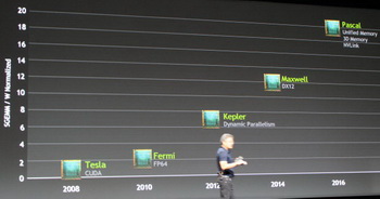
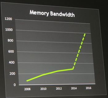
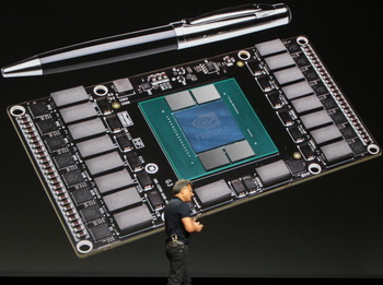
A year ago at a conference NVIDIA told about a hypothetical architecture Volt (Volta), which should be expected in 2016-2017 and which must first try to imagine 3D-memory HBM (High Bandwidth Memory). At today's conference, NVIDIA chief tactfully silent about solutions generation Volt, while the company's plans for 2016 appeared Pascal graphics cards with 3D-memory interface and new interprocessor NVLink. It can be assumed, that Volt will be postponed on a scale of priorities at a later date and will boast some innovative changes in architecture, while Pascal will be a combination of Maxwell, 3D-memory NVLink.  In yesterday's news, my colleague touched on the main points related to stack memory on the processor substrate and Pascal interface NVLink. As for the 3D-memory, NVIDIA has gone down the same path as AMD company . Actually, no other way. Memory HBM preparing for standardization committee JEDEC. Samples of high-density stack package chips using TSVs-compounds presented today all the leading manufacturers of memory, but still the same company Micron is busy promoting cubic HMC-memory, the South Korean company SK Hynix sent all their forces to promote a standard HBM-memory.  Due to the broadband interface HBM (h1024) data transfer rate between memory and the GPU Pascal on the substrate crystal can exceed three times the bandwidth, which we now see between GPU Kepler and GDDR5. Compared with the GPU Maxwell memory exchange speed by switching to 3D-memory can be doubled. As you can see, Pascal optionally have a new architecture to capture the imagination. It is important to note that the consumption of GPU will remain unchanged, which suggests a significant increase in energy efficiency.  Regarding interface NVLink. Overall NVLink coined for ligaments GPU NVIDIA composed of supercomputers for GPGPU-acceleration calculations. Prototype module Pascal, the company revealed that uses something like a standard server connector type mezzanine. However, in the future, the company expects to extend the use of NVLink also among discrete gaming graphics. Recall last summer NVIDIA and IBM entered into a strategic agreement on the establishment of a common computing ecosystem. It was also about licensing elements IBM Power architecture, NVIDIA and Google. So, NVLink. According to the company, this kind of productive alternative to PCI Express 3.0, which can speed 5-12 times surpass the regular interface. So far, however, the advantage NVLink looks modest. Eight lanes PCI Express 3.0 can collectively provide the exchange rate at 8 GB / s (8 Gb / s per lane). Related Products : | ||
|
|
||
|
xtreview is your : Video card - cpu - memory - Hard drive - power supply unit source |
|
|
|
|
||
|
Xtreview Support  N-Post:xxxx Xtreview Support        |
A LITTLE MORE DETAIL ABOUT NVIDIA NVLINK MEMORY AND 3D-PASCAL |
| Please Feel Free to write any Comment; Thanks  |
For the adventure game Little Nightmares announced just three additions (2017-06-08)
Female sex shows little interest in the helmet HTC Vive virtual reality (2017-02-28)
New trailer, unusual horror Little Nightamares (2017-01-18)
RuTracker ban has alittle impact on the attendance of the resource (2016-01-28)
Toyota believes that every driver in the future will get a little surveyor (2015-12-23)
External power for PlayStation VR will be a little less than Wii (2015-12-17)
GeForce GTX 750 is now also a little GeForce GTX 950 (2015-12-01)
Skylake will differ little from Haswell (2015-03-02)
Wearable devices collect little medical data (2014-10-26)
Smartphones have little effect on laptops buyers (2014-10-15)
ARM and TSMC introduced the industry first 16-nm FinFET-assembly with the use of technology Big.Little (2014-10-02)
Prior to the commencement of commercial production of graphene there still little time (2014-09-30)
Samsung has little interest in the notebook segment (2014-09-08)
At Computex 2014 to motherboards based on the Intel X99 will be paid little attention (2014-06-02)
Plextor talk little more about their updates in M6 (2014-05-29)
A little more detail about NVIDIA NVLink memory and 3D-Pascal (2014-03-26)
Laser fusion became a little closer (2014-02-15)
Prior to the publication of Radeon R9 290X reviews remain only a little more than a day (2013-10-23)
A little about the hardware side of the AMD TrueAudio (2013-10-09)
A little more about smart phones with a curved display (2013-10-08)
![]()
To figure out your best laptops .Welcome to XTreview.com. Here u can find a complete computer hardware guide and laptop rating .More than 500 reviews of modern PC to understand the basic architecture


7600gt review
7600gt is the middle card range.
We already benchmarked this video card and found that ...

 geforce 8800gtx and 8800gts
  Xtreview software download Section
  AMD TURION 64 X2 REVIEW
  INTEL PENTIUM D 920 , INTEL PENTIUM D 930
  6800XT REVIEW
  computer hardware REVIEW
  INTEL CONROE CORE DUO 2 REVIEW VS AMD AM2
  INTEL PENTIUM D 805 INTEL D805
  Free desktop wallpaper
  online fighting game
  Xtreview price comparison center
 Lastest 15 Reviews


Rss Feeds
Last News
- The new version of GPU-Z finally kills the belief in the miracle of Vega transformation
- The motherboard manufacturer confirms the characteristics of the processors Coffee Lake
- We are looking for copper coolers on NVIDIA Volta computing accelerators
- Unofficially about Intels plans to release 300-series chipset
- The Japanese representation of AMD offered monetary compensation to the first buyers of Ryzen Threadripper
- This year will not be released more than 45 million motherboards
- TSMC denies the presentation of charges from the antimonopoly authorities
- Radeon RX Vega 64 at frequencies 1802-1000 MHz updated the record GPUPI 1B
- AMD itself would like to believe that mobile processors Ryzen have already been released
- AMD Vega 20 will find application in accelerating computations
- Pre-orders for new iPhone start next week
- Radeon RX Vega 57, 58 and 59: the wonders of transformation
- ASML starts commercial delivery of EUV-scanners
- The older Skylake processors with a free multiplier are removed from production
- Meizu will release Android-smartphone based on Helio P40
- AMD Bristol Ridge processors are also available in American retail
- The fate of Toshiba Memory can be solved to the next environment
- duo GeForce GTX 1080 Ti in GPUPI 1B at frequencies of 2480-10320 MHz
- New Kentsfield overclocking record up to 5204 MHz
- Lenovo released Android-smartphone K8

HALO 3 HALO 3 - Final Fight!

PREY Prey is something you don t often see anymore: a totally unigue shooter experience.

computer news computer parts review Old Forum Downloads New Forum Login Join Articles terms Hardware blog Sitemap Get Freebies


