Samsung financed by the American laboratory for the development of 7-5 nm semiconductor
![]()
|
xtreview is your : Video card - cpu - memory - Hard drive - power supply unit source |
|
|||
|
|
||||

 Recommended : Free unlimited image hosting with image editor
|
POSTER: computer news || SAMSUNG FINANCED BY THE AMERICAN LABORATORY FOR THE DEVELOPMENT OF 7-5 NM SEMICONDUCTOR |
DATE:2014-08-31 |
|
|
According to the requirements of Samsung, it is necessary to create a technology that would combine traditional CMOS-process, FinFET-transistors and new materials of the III-V of the periodic table. First of all, it's a combination of gallium arsenide and indium. Such materials prevent leaks and cross-contamination must be applied to the buffer layer rather than directly on the substrate. It should be borne in mind that the group III-V allow you to create n-transitions to move the electrons, while for p-transitions of these materials of little use. 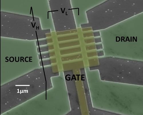 The developers are also involved in the practical side of the issue. The next step will be the release of elements using 30-nm process technology . The structure of transistors, by the way, a rather unique and involves the use of five vertical gates within each transistor. The electron mobility transistor with the gate of the elements of groups III-V as assessed in the prototype 2-3 fold compared to traditional silicon. The effect will be to increase with a decrease in process technology, where silicon will stop working. This is to be expected at lower production scale, 5 to 7 nm. All rights to the development, by the way, will be owned by Samsung. If developers will succeed, the company will be able to upgrade their factory for the production of semiconductors in the new environment. Related Products : | ||
|
|
||
|
xtreview is your : Video card - cpu - memory - Hard drive - power supply unit source |
|
|
|
|
||
|
Xtreview Support  N-Post:xxxx Xtreview Support  |
SAMSUNG FINANCED BY THE AMERICAN LABORATORY FOR THE DEVELOPMENT OF 7-5 NM SEMICONDUCTOR |
| Please Feel Free to write any Comment; Thanks  |
Development of The Banner Saga 3 financed prematurely (2017-01-31)
Samsung financed by the American laboratory for the development of 7-5 nm semiconductor (2014-08-31)
![]()
To figure out your best laptops .Welcome to XTreview.com. Here u can find a complete computer hardware guide and laptop rating .More than 500 reviews of modern PC to understand the basic architecture


7600gt review
7600gt is the middle card range.
We already benchmarked this video card and found that ...
 geforce 8800gtx and 8800gts Xtreview software download Section AMD TURION 64 X2 REVIEW INTEL PENTIUM D 920 , INTEL PENTIUM D 930 6800XT REVIEW computer hardware REVIEW INTEL CONROE CORE DUO 2 REVIEW VS AMD AM2 INTEL PENTIUM D 805 INTEL D805 Free desktop wallpaper online fighting game Xtreview price comparison center
Rss Feeds

- The new version of GPU-Z finally kills the belief in the miracle of Vega transformation
- The motherboard manufacturer confirms the characteristics of the processors Coffee Lake
- We are looking for copper coolers on NVIDIA Volta computing accelerators
- Unofficially about Intels plans to release 300-series chipset
- The Japanese representation of AMD offered monetary compensation to the first buyers of Ryzen Threadripper
- This year will not be released more than 45 million motherboards
- TSMC denies the presentation of charges from the antimonopoly authorities
- Radeon RX Vega 64 at frequencies 1802-1000 MHz updated the record GPUPI 1B
- AMD itself would like to believe that mobile processors Ryzen have already been released
- AMD Vega 20 will find application in accelerating computations
- Pre-orders for new iPhone start next week
- Radeon RX Vega 57, 58 and 59: the wonders of transformation
- ASML starts commercial delivery of EUV-scanners
- The older Skylake processors with a free multiplier are removed from production
- Meizu will release Android-smartphone based on Helio P40
- AMD Bristol Ridge processors are also available in American retail
- The fate of Toshiba Memory can be solved to the next environment
- duo GeForce GTX 1080 Ti in GPUPI 1B at frequencies of 2480-10320 MHz
- New Kentsfield overclocking record up to 5204 MHz
- Lenovo released Android-smartphone K8


computer news computer parts review Old Forum Downloads New Forum Login Join Articles terms Hardware blog Sitemap Get Freebies