OOPS! You forgot to upload swfobject.js ! You must upload this file for your form to work.
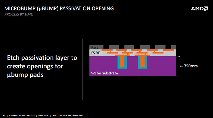
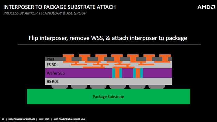
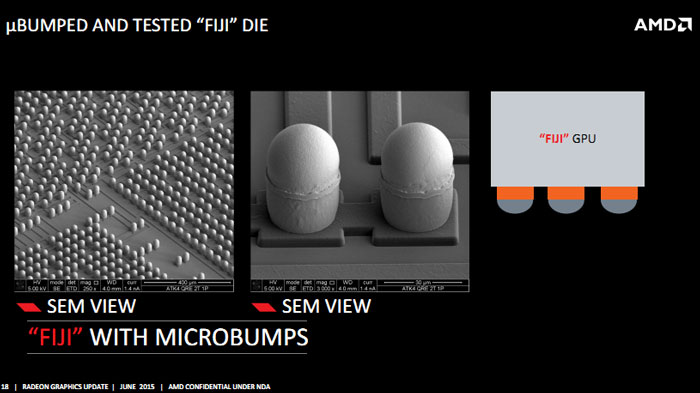
The manufacturing and packaging Bridge GPU Fiji and HBM memory
![]()
|
xtreview is your : Video card - cpu - memory - Hard drive - power supply unit source |
|
|||
|
|
||||
 Recommended : Free unlimited image hosting with image editor
|
xtreview is your : Video card - cpu - memory - Hard drive - power supply unit source |
|
|
|
|
||
|
Xtreview Support  N-Post:xxxx Xtreview Support        |
THE MANUFACTURING AND PACKAGING BRIDGE GPU FIJI AND HBM MEMORY |
| Please Feel Free to write any Comment; Thanks  |
Samsung is determined to narrow the gap with TSMC in the contract manufacturing market (2017-07-25)
On the prospects of contract manufacturing Samsung (2017-05-17)
Samsung sub-division for semiconductor manufacturing contract has gained relative autonomy (2017-05-14)
Samsung may separate the business of manufacturing semiconductor devices (2016-12-15)
TSMC is preparing to build a manufacturing facility for the production of 3-nm products (2016-12-07)
China hopes to enter the top ten countries on the use of robots in manufacturing (2016-07-25)
Xiaomi start manufacturing laptops in the first quarter of 2016 (2015-10-26)
Started mass production of 16-nm manufacturing at TSMC (2015-07-18)
The manufacturing and packaging Bridge GPU Fiji and HBM memory (2015-06-18)
The manufacturing process of the metal case of Android-smartphone Samsung Galaxy Alpha (2014-08-23)
Intel disclaims manufacturing mobile and server processors Ivy Bridge (2014-07-17)
TSMC began manufacturing A8 processors (2014-03-06)
TSMC denies interest in buying the business of IBM processors manufacturing (2014-02-10)
Sony officially separates the business of manufacturing notebooks (2014-02-06)
In the area of contract chips manufacturing Intel is ready to turn to competitors (2013-11-22)
The manufacturing process of electronic devices enclosures becomes more difficult (2013-06-16)
Fujitsu selling semiconductor manufacturing business (2013-05-01)
Intel says its own principles in the field of contract manufacturing (2013-04-19)
Samsung is ready to work closely with NVIDIA in the field of contract processors manufacturing (2013-04-11)
Renesas seeking a buyer for the business of manufacturing platforms for phones (2013-03-22)
![]()
To figure out your best laptops .Welcome to XTreview.com. Here u can find a complete computer hardware guide and laptop rating .More than 500 reviews of modern PC to understand the basic architecture


7600gt review
7600gt is the middle card range.
We already benchmarked this video card and found that ...

 geforce 8800gtx and 8800gts
  Xtreview software download Section
  AMD TURION 64 X2 REVIEW
  INTEL PENTIUM D 920 , INTEL PENTIUM D 930
  6800XT REVIEW
  computer hardware REVIEW
  INTEL CONROE CORE DUO 2 REVIEW VS AMD AM2
  INTEL PENTIUM D 805 INTEL D805
  Free desktop wallpaper
  online fighting game
  Xtreview price comparison center
 Lastest 15 Reviews


Rss Feeds
Last News
- The new version of GPU-Z finally kills the belief in the miracle of Vega transformation
- The motherboard manufacturer confirms the characteristics of the processors Coffee Lake
- We are looking for copper coolers on NVIDIA Volta computing accelerators
- Unofficially about Intels plans to release 300-series chipset
- The Japanese representation of AMD offered monetary compensation to the first buyers of Ryzen Threadripper
- This year will not be released more than 45 million motherboards
- TSMC denies the presentation of charges from the antimonopoly authorities
- Radeon RX Vega 64 at frequencies 1802-1000 MHz updated the record GPUPI 1B
- AMD itself would like to believe that mobile processors Ryzen have already been released
- AMD Vega 20 will find application in accelerating computations
- Pre-orders for new iPhone start next week
- Radeon RX Vega 57, 58 and 59: the wonders of transformation
- ASML starts commercial delivery of EUV-scanners
- The older Skylake processors with a free multiplier are removed from production
- Meizu will release Android-smartphone based on Helio P40
- AMD Bristol Ridge processors are also available in American retail
- The fate of Toshiba Memory can be solved to the next environment
- duo GeForce GTX 1080 Ti in GPUPI 1B at frequencies of 2480-10320 MHz
- New Kentsfield overclocking record up to 5204 MHz
- Lenovo released Android-smartphone K8

HALO 3 HALO 3 - Final Fight!

PREY Prey is something you don t often see anymore: a totally unigue shooter experience.

computer news computer parts review Old Forum Downloads New Forum Login Join Articles terms Hardware blog Sitemap Get Freebies


