OOPS! You forgot to upload swfobject.js ! You must upload this file for your form to work.
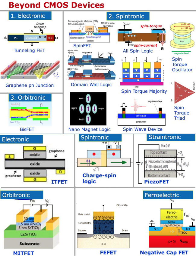
Intel life outside the traditional CMOS process technology
![]()
|
xtreview is your : Video card - cpu - memory - Hard drive - power supply unit source |
|
|||
|
|
||||
 Recommended : Free unlimited image hosting with image editor
|
xtreview is your : Video card - cpu - memory - Hard drive - power supply unit source |
|
|
|
|
||
|
Xtreview Support  N-Post:xxxx Xtreview Support        |
INTEL LIFE OUTSIDE THE TRADITIONAL CMOS PROCESS TECHNOLOGY |
| Please Feel Free to write any Comment; Thanks  |
AMD counts on the long life of the 7-nm process technology (2017-07-25)
For the original Half-Life was released an official patch (2017-07-11)
The new season of Life is Strange starts at the end of summer (2017-06-12)
Technological standards of 7 nm will give life to two generations of graphics solutions AMD (2017-06-08)
Ilon Mask is ready to dedicate Tesla for the rest of his life (2017-05-05)
Intel life outside the traditional CMOS process technology (2017-04-04)
Bay Trail processors stepping B3 end of life (2017-02-13)
TSMC will implement EUV lithography is only the second year of life, 7-nm process technology (2017-01-13)
Half-Life 3 can be real-time strategy (2017-01-09)
The first image of Xena fan-remake of Half-Life Black Mesa (2016-12-22)
Blu Life Max:budget smartphone with 3700 mAh battery (2016-12-20)
Gamers have decided to nominate the Half-Life 2 Episode Two on Steam-premium game worthy continuation (2016-11-25)
Huawei has introduced affordable Fit fitness tracker with long battery life (2016-11-04)
Robocar Mercedes-Benz will give priority to the life of the driver, not a pedestrian (2016-10-18)
Vega 10 give life and dual-processor graphics cards (2016-10-06)
Fuze Case is designed to return the iPhone 7 audio jack and extend battery life (2016-10-04)
HTC introduced Desire Desire 10 Pro and Lifestyle 10 September 20 (2016-09-13)
HTC Desire 10 and Desire Lifestyle 10 Pro debut September 20 (2016-09-01)
In September, HTC will introduce Desire Lifestyle 10 and Desire Pro 10 (2016-08-14)
The growing popularity of OLED displays inhales in Japanese companies more life (2016-06-16)
![]()
To figure out your best laptops .Welcome to XTreview.com. Here u can find a complete computer hardware guide and laptop rating .More than 500 reviews of modern PC to understand the basic architecture


7600gt review
7600gt is the middle card range.
We already benchmarked this video card and found that ...

 geforce 8800gtx and 8800gts
  Xtreview software download Section
  AMD TURION 64 X2 REVIEW
  INTEL PENTIUM D 920 , INTEL PENTIUM D 930
  6800XT REVIEW
  computer hardware REVIEW
  INTEL CONROE CORE DUO 2 REVIEW VS AMD AM2
  INTEL PENTIUM D 805 INTEL D805
  Free desktop wallpaper
  online fighting game
  Xtreview price comparison center
 Lastest 15 Reviews


Rss Feeds
Last News
- The new version of GPU-Z finally kills the belief in the miracle of Vega transformation
- The motherboard manufacturer confirms the characteristics of the processors Coffee Lake
- We are looking for copper coolers on NVIDIA Volta computing accelerators
- Unofficially about Intels plans to release 300-series chipset
- The Japanese representation of AMD offered monetary compensation to the first buyers of Ryzen Threadripper
- This year will not be released more than 45 million motherboards
- TSMC denies the presentation of charges from the antimonopoly authorities
- Radeon RX Vega 64 at frequencies 1802-1000 MHz updated the record GPUPI 1B
- AMD itself would like to believe that mobile processors Ryzen have already been released
- AMD Vega 20 will find application in accelerating computations
- Pre-orders for new iPhone start next week
- Radeon RX Vega 57, 58 and 59: the wonders of transformation
- ASML starts commercial delivery of EUV-scanners
- The older Skylake processors with a free multiplier are removed from production
- Meizu will release Android-smartphone based on Helio P40
- AMD Bristol Ridge processors are also available in American retail
- The fate of Toshiba Memory can be solved to the next environment
- duo GeForce GTX 1080 Ti in GPUPI 1B at frequencies of 2480-10320 MHz
- New Kentsfield overclocking record up to 5204 MHz
- Lenovo released Android-smartphone K8

HALO 3 HALO 3 - Final Fight!

PREY Prey is something you don t often see anymore: a totally unigue shooter experience.

computer news computer parts review Old Forum Downloads New Forum Login Join Articles terms Hardware blog Sitemap Get Freebies


