The GeForce GTX 670 officially announced

|
xtreview is your : Video card - cpu - memory - Hard drive - power supply unit source |
|
|||
|
|
||||


 Recommended : Free unlimited image hosting with image editor
|
POSTER: computer news || THE GEFORCE GTX 670 OFFICIALLY ANNOUNCED |
DATE:2012-05-10 |
|
|
The past week has been rich in revelations about the video card GeForce GTX 670, and each day we were able to study the appearance of products prepared for the announcement by NVIDIA partners. Today, the GeForce GTX 670 has been officially presented. 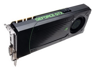 Here's the GeForce GTX 670 reference design. The length of PCB is 240 mm. NVIDIA partners will offer enough products of their own design. 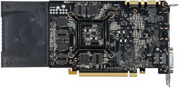 The cooling system fan was borrowed from the GeForce GTX 680. The radiator of GeForce GTX 670 has a rather primitive design: heat pipes could not be found. This cooling system is not characterized by high noise levels, even after overclocking. For the power supply the card is connected via two six-connectors, power supply unit used shall be not less than 500 watts. Memory chips like GDDR5, forming a total volume of 2 GB and 256-bit bus, located on both sides of the PCB. 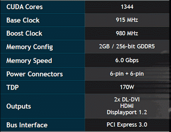 Frequency are equal to 915/6008 MHz, GPU Boost mode the core frequency go up to 980 MHz. The GeForce GTX 670 use the same GPU GK104, which was used in GeForce GTX 680 and GeForce GTX 690. It was released on 28 nm technology, and contains 3.54 million transistors. The number of stream processors is reduced from 1536 to 1344 units, the number of texture units is equal to 112 pieces , the number of ROP units remained equal to 32 pieces. Power consumption does not exceed 170 watts, typical power consumption is equal to 141 w .The rear panel has two ports, Dual-Link DVI, HDMI and full-size DisplayPort 1.2. The recommended value of GeForce GTX 670 in the U.S. market is $ 399. Many NVIDIA partners will be offering overclocked versions of GeForce GTX 670 running at over 1 GHz core . Related Products : | ||
|
|
||
|
xtreview is your : Video card - cpu - memory - Hard drive - power supply unit source |
|
|
|
|
||
|
Xtreview Support  N-Post:xxxx Xtreview Support  |
THE GEFORCE GTX 670 OFFICIALLY ANNOUNCED |
| Please Feel Free to write any Comment; Thanks  |
duo GeForce GTX 1080 Ti in GPUPI 1B at frequencies of 2480-10320 MHz (2017-09-07)
The GeForce GTX 1080 Ti at the frequencies 2657-10008 MHz took the third place in GPUPI 1B (2017-09-04)
The length of the video card GeForce GTX 1080 in the Gigabyte version does not exceed 169 mm (2017-09-04)
dual-processor video card GeForce GTX 560 Ti x2 (2017-08-27)
Sixteen Skylake-X cores and four GeForce GTX 1080 Ti a couple of fresh records (2017-08-23)
GeForce GTX 1080 Ti was able to overclock to 2898 MHz on the chip (2017-08-15)
The creator of one of the fastest GeForce GTX 1080 Ti shared the secrets of overclocking (2017-08-15)
The world record Unigine Heaven Xtreme is updated with the help of Core i7-7740X and GeForce GTX 1080 Ti (2017-08-14)
Kaby Lake and GeForce GTX 1080 Ti update the absolute world record 3DMark2001 SE (2017-08-10)
GeForce GTX 1080 Ti at frequencies of 2630-12888 MHz distinguished itself in 3DMark Time Spy (2017-08-07)
Revenge duo GeForce GTX 1080 Ti in 3DMark Vantage Performance was accompanied by lower frequencies (2017-08-07)
Paired video cards GeForce GTX 1080 Ti updated world record 3DMark Vantage Performance (2017-08-04)
The duo Skylake-X and GeForce GTX 1080 Ti managed to update the record of 3DMark Vantage Performance (2017-08-03)
Core i9-7900X at a frequency of 6.0 GHz was adjacent to the overclocked to 2607 MHz on the GeForce GTX 1080 Ti chip (2017-08-02)
GeForce GTX 1080 Ti and Kaby Lake-X have distinguished themselves in Unigine Heaven Xtreme (2017-08-01)
Core i9-7900X helped in overclocking GeForce GTX 750 (2017-07-31)
Kaby Lake-X and GeForce GTX 1080 Ti have updated the world record 3DMark03 (2017-07-21)
Radeon RX Vega in Budapest challenged the GeForce GTX 1080 (2017-07-19)
GeForce GTX 1080 Ti on the frequency of the chip 2632 MHz has updated the records 3DMark Fire Strike (2017-07-19)
Greek overclocker overclocked GeForce GTX 1080 Ti to 2645 MHz on chip (2017-07-19)

To figure out your best laptops .Welcome to XTreview.com. Here u can find a complete computer hardware guide and laptop rating .More than 500 reviews of modern PC to understand the basic architecture


7600gt review
7600gt is the middle card range.
We already benchmarked this video card and found that ...
 geforce 8800gtx and 8800gts Xtreview software download Section AMD TURION 64 X2 REVIEW INTEL PENTIUM D 920 , INTEL PENTIUM D 930 6800XT REVIEW computer hardware REVIEW INTEL CONROE CORE DUO 2 REVIEW VS AMD AM2 INTEL PENTIUM D 805 INTEL D805 Free desktop wallpaper online fighting game Xtreview price comparison center
Rss Feeds


- The new version of GPU-Z finally kills the belief in the miracle of Vega transformation
- The motherboard manufacturer confirms the characteristics of the processors Coffee Lake
- We are looking for copper coolers on NVIDIA Volta computing accelerators
- Unofficially about Intels plans to release 300-series chipset
- The Japanese representation of AMD offered monetary compensation to the first buyers of Ryzen Threadripper
- This year will not be released more than 45 million motherboards
- TSMC denies the presentation of charges from the antimonopoly authorities
- Radeon RX Vega 64 at frequencies 1802-1000 MHz updated the record GPUPI 1B
- AMD itself would like to believe that mobile processors Ryzen have already been released
- AMD Vega 20 will find application in accelerating computations
- Pre-orders for new iPhone start next week
- Radeon RX Vega 57, 58 and 59: the wonders of transformation
- ASML starts commercial delivery of EUV-scanners
- The older Skylake processors with a free multiplier are removed from production
- Meizu will release Android-smartphone based on Helio P40
- AMD Bristol Ridge processors are also available in American retail
- The fate of Toshiba Memory can be solved to the next environment
- duo GeForce GTX 1080 Ti in GPUPI 1B at frequencies of 2480-10320 MHz
- New Kentsfield overclocking record up to 5204 MHz
- Lenovo released Android-smartphone K8












computer news computer parts review Old Forum Downloads New Forum Login Join Articles terms Hardware blog Sitemap Get Freebies


