OOPS! You forgot to upload swfobject.js ! You must upload this file for your form to work.
Found a way to create band gaps in graphene
![]()
|
xtreview is your : Video card - cpu - memory - Hard drive - power supply unit source |
|
|||
|
|
||||
 Recommended : Free unlimited image hosting with image editor
|
POSTER: computer news || FOUND A WAY TO CREATE BAND GAPS IN GRAPHENE |
DATE:2012-11-27 |
|
|
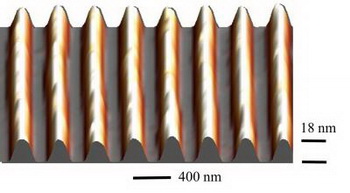
Scientists from Georgia Institute of Technology have developed a way to create band gaps in graphene by creating curves on the surface of the substrate. The process begins with etching using electron beams grooves on a silicon wafer. Then the modified surface thus applied the heated carbon, which is hitting the silicon crystallizes in the form of strips of graphene.  The study of the electronic properties of the resulting material has led to an important conclusion: the curved portion has a forbidden band, which has the properties of a semiconductor. Thus, depending on the topography of substrate, a single sheet of graphene may be conductive and semiconductor area.
Scientists have yet to find a full explanation of the processes that cause the graphene to assume the role of semiconductor, however, this does not diminish the significance of the research. Related Products : | ||
|
|
||
|
xtreview is your : Video card - cpu - memory - Hard drive - power supply unit source |
|
|
|
|
||
|
Xtreview Support  N-Post:xxxx Xtreview Support        |
FOUND A WAY TO CREATE BAND GAPS IN GRAPHENE |
| Please Feel Free to write any Comment; Thanks  |
The new version of GPU-Z finally kills the belief in the miracle of Vega transformation (2017-09-08)
The motherboard manufacturer confirms the characteristics of the processors Coffee Lake (2017-09-08)
We are looking for copper coolers on NVIDIA Volta computing accelerators (2017-09-08)
Unofficially about Intels plans to release 300-series chipset (2017-09-08)
The Japanese representation of AMD offered monetary compensation to the first buyers of Ryzen Threadripper (2017-09-08)
This year will not be released more than 45 million motherboards (2017-09-08)
TSMC denies the presentation of charges from the antimonopoly authorities (2017-09-08)
Radeon RX Vega 64 at frequencies 1802-1000 MHz updated the record GPUPI 1B (2017-09-08)
AMD itself would like to believe that mobile processors Ryzen have already been released (2017-09-08)
AMD Vega 20 will find application in accelerating computations (2017-09-08)
Pre-orders for new iPhone start next week (2017-09-07)
Radeon RX Vega 57, 58 and 59: the wonders of transformation (2017-09-07)
ASML starts commercial delivery of EUV-scanners (2017-09-07)
The older Skylake processors with a free multiplier are removed from production (2017-09-07)
Meizu will release Android-smartphone based on Helio P40 (2017-09-07)
AMD Bristol Ridge processors are also available in American retail (2017-09-07)
The fate of Toshiba Memory can be solved to the next environment (2017-09-07)
duo GeForce GTX 1080 Ti in GPUPI 1B at frequencies of 2480-10320 MHz (2017-09-07)
Lenovo released Android-smartphone K8 (2017-09-07)
Advertising Radeon RX 570 for 279 dollars AMD caused a storm of emotions (2017-09-07)
![]()
To figure out your best laptops .Welcome to XTreview.com. Here u can find a complete computer hardware guide and laptop rating .More than 500 reviews of modern PC to understand the basic architecture


7600gt review
7600gt is the middle card range.
We already benchmarked this video card and found that ...

 geforce 8800gtx and 8800gts
  Xtreview software download Section
  AMD TURION 64 X2 REVIEW
  INTEL PENTIUM D 920 , INTEL PENTIUM D 930
  6800XT REVIEW
  computer hardware REVIEW
  INTEL CONROE CORE DUO 2 REVIEW VS AMD AM2
  INTEL PENTIUM D 805 INTEL D805
  Free desktop wallpaper
  online fighting game
  Xtreview price comparison center
 Lastest 15 Reviews


Rss Feeds
Last News
- The new version of GPU-Z finally kills the belief in the miracle of Vega transformation
- The motherboard manufacturer confirms the characteristics of the processors Coffee Lake
- We are looking for copper coolers on NVIDIA Volta computing accelerators
- Unofficially about Intels plans to release 300-series chipset
- The Japanese representation of AMD offered monetary compensation to the first buyers of Ryzen Threadripper
- This year will not be released more than 45 million motherboards
- TSMC denies the presentation of charges from the antimonopoly authorities
- Radeon RX Vega 64 at frequencies 1802-1000 MHz updated the record GPUPI 1B
- AMD itself would like to believe that mobile processors Ryzen have already been released
- AMD Vega 20 will find application in accelerating computations
- Pre-orders for new iPhone start next week
- Radeon RX Vega 57, 58 and 59: the wonders of transformation
- ASML starts commercial delivery of EUV-scanners
- The older Skylake processors with a free multiplier are removed from production
- Meizu will release Android-smartphone based on Helio P40
- AMD Bristol Ridge processors are also available in American retail
- The fate of Toshiba Memory can be solved to the next environment
- duo GeForce GTX 1080 Ti in GPUPI 1B at frequencies of 2480-10320 MHz
- New Kentsfield overclocking record up to 5204 MHz
- Lenovo released Android-smartphone K8

HALO 3 HALO 3 - Final Fight!

PREY Prey is something you don t often see anymore: a totally unigue shooter experience.

computer news computer parts review Old Forum Downloads New Forum Login Join Articles terms Hardware blog Sitemap Get Freebies


