DDR3 REVIEW , BENCHMARK , TECHNICAL INFORMATION AND DDR2 COMPARISON
![]()
|
|
 |
|||||||||||||||||||||||||||||||||||||||||||||||||||||||||||||||||||||||||||||||
| Posted:2007-05-19 By memory review Number of View:58083 |
||||||||||||||||||||||||||||||||||||||||||||||||||||||||||||||||||||||||||||||||
By :memory review Posted:2007-05-19
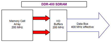
The first evolutionary jump in DDR SDRAM memory technologies development was the passage from DDR to DDR2. The first DDR models functioned at 100 MHz (frequency) only (they had a DDR-200 rating ), then frequency gradually increased to 200 MHz (DDR-400). Their was a simultaneous decrease in latency : the initial latency diagrams was updated from 3- 3- 3-8 to lower value 2-2-2-5. Then appeared high-frequency memory modules DDR (up to 300 MHz, ( DDR-600 ) ); however, officially they were not accepted by JEDEC standard . The increase in memory module frequency , or reduction in latency required increase in voltage from the standard level 2.5 v up to 2.85 v. When a further increase in memory clock frequencies ( DDR ) proved to be practically impossible, on desktop market appeared new operational memory , second generation memory DDR SDRAM : DDR2, which gradually began to prove its competitive ability. Initial DDR2 versions were presented by 200 MHz frequencies (DDR 2-400) and 266 MHz (DDR 2-533) in other words, DDR2 began its development, where (officially) finished the DDR development . Moreover, initial standard DDR2 provided higher frequency versions, in comparison with customary DDR : as 333- MHz modules DDR 2-667 and 400- MHz version DDR 2-800. In this case DDR2 microcircuits were based in the new technological process, which allow to use 1.8 v only (which was one of the main factors in the energy consumption reduction ) and also allowed to reach higher capacities . But how DDR2 memory with high clock frequencies result in simultaneous decrease of its energy consumption, in comparison with DDR? What are the DDR2 advantages over DDR, is there some deficiencies? In order to answer to these questions,we have made this review. For beginning, let us examine the maximally simplified diagram of DDR functioning memory .
The data transmission from memory module microcircuits to memory controller on external system bus is accomplished on both half-periods of sync signal . In this consists the technology double data rate, precisely due to this last the rating, or effective DDR memory frequency is always doubled (for example, DDR-400 with 200- MHz external system bus frequency ). Thus, effective frequency of the external system bus to the memory DDR-400 is 400 MHz, whereas its true frequency, or input-output buffers frequency is only 200 MHz. In memory devices , first generation DDR , the internal frequency of memory microcircuits was equal to the true external system bus frequency (to frequency of buffers input-output) . In other words, it is possible to say that with equal conditions the internal system bus is doubly wider in comparison with external system bus .
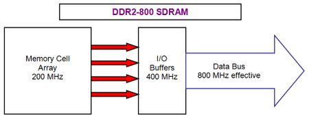
The most natural solution to reach higher clock frequencies with transfer from DDR to DDR2 was reduction in the clock frequency of internal system bus with respect to the real clock frequency of external system bus . So, in the example of DDR memory microcircuits , input-output buffers frequencies are 400 MHz, and effective external system frequency is 800 MHz (since the technology double data rate remains valid ). In this case the frequency of internal system bus is only 200 MHz; therefore for 1 bits transfer (for each data line ) the external system bus witch work with the effective frequency 800 MHz on each 200- MHz , the internal system bus transfer already 4 bits data . In other words, the internal system bus in DDR2 memory microcircuit is 4 times wider in comparison with its external system bus. This diagram of data access , realized in DDR2, is called diagram (4n-prefetch). Its advantages over diagram 2n-prefetch, realized in DDR, are obvious. From one side, for achieving equal bandwidth it is possible to use doubly smaller internal frequency of memory microcircuits (200 MHz for DDR-400 and only 100 MHz for DDR 2-400, this also allow to considerably decrease the energy consumption). From other side, with equal internal frequency the DDR and DDR2 microcircuits (200 MHz for DDR-400 and DDR 2-800) this last will be twice larger in theoretical bandwidth. But what about deficiencies ?. the DDR2 microcircuits at the doubly smaller frequency use more complex circuit ( conversion 4-1 ) witch leads in growth in latency, this was observed in practice with the first models DDR2 memory module . Further development of DDR2 memory technology was analogous to the development of its previous generation. They achieved 333 and 400 MHz frequency (they were realized in official standards DDR 2-667 and DDR 2-800). Latency were considerably lowered, officially appeared new JEDEC standard version (JESD79-2b), which allows to reduce latency from 4- 4-4 to 3- 3-3 for DDR 2-533, from 5-5-5 to 4- 4-4 for DDR 2-667, from 6- 6-6 to to 5- 5-5 and even 4- 4-4 for DDR 2-800. Certainly, appeared as in the case of DDR the nonstandard DDR2 version , its frequency was higher than the limits of JEDEC specification : up to 625 MHz (DDR 2-1250) with latency 5-5-5, or standard DDR 2-800, but with extremely low latency like 3- 3-3. As before, for achieving such rate , producer made a significant increase in modules voltage from standard level 1.8 v up to extremely high levels on the order of 2.4 v (which is a bit inferior to the standard value of previous generation DDR memory : 2.5 v). As it became clear , producer placed more advanced methods of heat removal from memory microcircuits , in some case their used even a external active cooling. As in the case with past generation DDR memory , today we have reached the limit of DDR2 memory technology . Therefore its completely regular to expect another evolutionary jump , with passage from DDR2 memory to the new DDR3 standard .
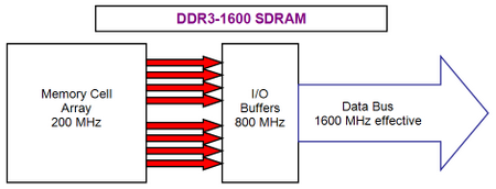
As is it clear from the picture passage from DDR2 to DDR3, exactly repeats the examined above idea, placed in the transfer from DDR to DDR2. the data transmission as before is accomplished on both half-periods of sync signal at the doubled effective frequency relative to the natural memory system bus frequency . Here the performance ratings grew by 2, in comparison with DDR2 , the typical high-speed categories of new standard memory DDR3 will be version from DDR 3-800 to DDR 3-1600. A sequential increase in the theoretical bandwidth of memory components by 2 times is connected with reduction in their internal frequency . Therefore , for achieving the data transmission rate 1 bits/time for each line of the external system bus with effective frequency 1600 MHz , the utilized 200- MHz microcircuits will transfer 8 bits data per clock . the width of internal system bus prove to be 8 times more in comparison with the width of their external system bus. Obviously, this transmission diagram of type ( 8-1 ) will be called (8n-prefetch). Advantages with transfer from DDR2 to DDR3 will be the same as transfer from DDR to DDR2: from one side, reduction in energy consumption (DDR 3-800 against DDR 2-800), from other side , their a possibility of further growth in clock frequency . We have as in DDR2 the same deficiencies : further break between internal and external system bus frequency will lead in larger latency. DDR3: technical informationStandard DDR3 today is not accepted BY JEDEC, its adoption is expected nearer to the middle of the present year . Therefore the presented below information about the microcircuits and memory module DDR3 has only the preliminary nature. Let us begin from DDR3 memory microcircuits , whose first prototypes were declared in 2005. The accessible today DDR3 microcircuits models are based on 90 nm technological process and are characterized by voltage 1.5 v, which makes approximately 30% reduction in the power of DDR3 in comparison with DDR2 microcircuits (having standard voltage 1.8 v). Total reduction in the energy consumption in comparison with equivalent frequency DDR2 reaches approximately 40%, which is especially important for mobile systems. The capacities of components, provided by JEDEC specifications , vary from 512 Mbit to 8 Gbit, whereas the typical produced until today microcircuits have a bandwidth from 1 to 4 Gbit. The theoretical bandwidth of DDR3 microcircuits is twice higher in comparison with DDR2 due to the 8n-prefetch (against 4n-prefetch in DDR2). The quantity of logical banks in DDR3 microcircuits is also twice higher in comparison with typical value for DDR2 (4 banks), which theoretically allow to increase parallelism and hide some latency , connected with memory (tRP). Microcircuits DDR3 has FBGA- packing, which possesses a number of improvements in comparison with DDR2:
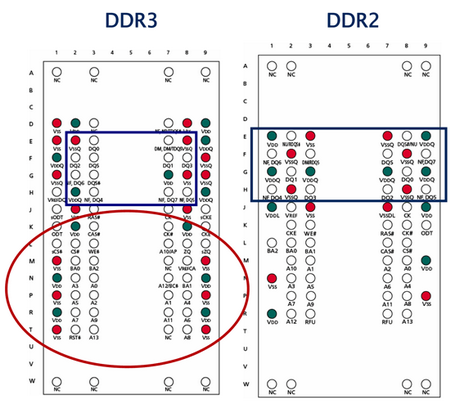 Fig. 4. microcircuits DDR3 and DDR2 Let us pass to the examination of DDR3 memory module . Like DDR2 memory module , they are released in the form of 240- contact printed-circuit board (120 contacts for each module side ); however, DDR3 is not electrically compatible with DDR2 .
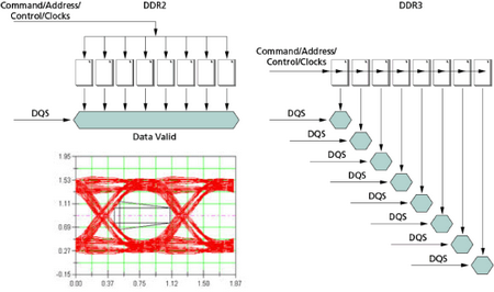
The distinctive special feature in technology design of DDR3 memory module is the application of (transient) (fly-by) architecture in the transfer of addresses and commands, and also the signals control and clock frequency of separate memory microcircuits with external signals (using resistor, located on memory module ). Schematically this architecture is represented in the next picture. This allow to attain increase in the quality of signals transfer , which is necessary for components functioning with high frequencies.
The difference between the method of addresses supply and commands, control signals and clock frequency in DDR2 and DDR3 memory module is represented in the next picture. . In DDR2 memory module the addresses supply and commands is accomplished in parallel to all module microcircuits , for example, in read case, all eight bit elements will prove to be accessible at the same moment (after the supply of the corresponding commands and the expiration of the corresponding delays) and memory controller will be able to simultaneously read all 64 bits data . At the same time, in DDR3 memory module as a result of transient architecture application , the addresses supply and commands ,each microcircuits obtains commands and addresses with specific delay relative to the previous microcircuit; therefore data elements , which correspond to the specific microcircuit, will also prove to be accessible with a certain delay relative to the data elements , which correspond to the previous microcircuit , which composes the physical memory module bank. To minimize delays, in DDR3 memory module , in comparison with DDR2 modules , are realized different interaction of memory controller with the system bus of memory module . It is called (read/write leveling) and this allow the memory controller to use a specific time with the data transmission method, that corresponds to the delay of entering addresses and commands (and consequently, data) in the specific module microcircuit .
Let us examine the speed characteristics of the assumed specifications for DDR3 memory module , which are presented in Table 1. Table 1. The speed characteristics of memory module DDR3
DDR3 Memory module will be proposed in versions from DDR 3-800 to DDR 3-1600 , But we do not exclude the appearance of high-speed modules categories DDR 3-1866. DDR3 memory module performance rating has a value in the form OF PC 3- X, where the X indicates the bandwidth of module in single-channel regime, expressed in MB./s . Since DDR3 memory module have the same length as DDR2 memory module (64 bits), numerical rating values for DDR2 and DDR3 coincide (for example, PC 2-6400 for DDR 2-800 and PC 3-6400 for DDR 3-800). The typical latency, assumed at present for DDR3 memory , appear very imposing (for example, 9 9-9 for DDR 3-1600); however, We note that high relative latency values being transferred in the absolute values (in nanoseconds), taking in account the smaller cycle time in DDR3 this value become acceptable. For example, signal latency CAS # (tCL) for memory module DDR 3-800 with latency 6-6-6 -15 ns, is certainly bigger in comparison with typical DDR 2-800 latency 5-5-5, for which tCL is 12.5 ns. At the same time, DDR 3-1600 with latency 9 9-9 has already been characterized by tCL 11.25 ns, which is located on DDR 2-533 level , this is sufficiently low delays (as latency 3- 3-3). Moreover, we note that further latency reduction will be added in proportion to technology development as in case of DDR2 . Test Configuration
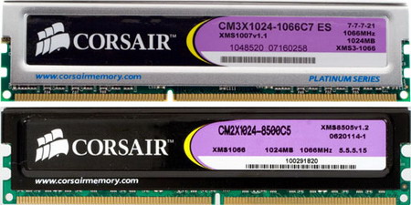
 MSI p35 neo combo DDR3: the first results : real testingLet us pass, from theory to practice. At our disposal proved to be the pre-series models motherboard MSI p35 neo combo, based on new chipset Intel p35 and memory modules corsair XMS 3-1066 (CM3X1024-1066C7 ES). The motherboard MSI p35 neo combo, as it is clear from the name, is the combined version. it allow to install both memory module DDR2 and DDR3. Let us note that memory module in this motherboard work only with one module Type either DDR2 or DDR3. the simultaneous use of DDR2 memory module and DDR3 is impossible. Memory module CM3X1024-1066C7 ES are engineering model DDR 3-1066 with latency 7-7-7-21.. From the present generation DDR2 memory module we selected the memory corsair DOMINATOR XMS 2-9136C5D witch approximately equal in frequency (DDR 2-1142), this memory was used in regime DDR 2-1066 with default latency 5-5-5-15. The functioning regime of DDR2 memory module and latencies were set manually in BIOS setup , the voltage was increased to 2.3 v. let us note that the current BIOS version (V1.0B16 20.04.2007) for motherboard MSI p35 neo combo does not allow to properly set the memory latency in DDR3 module , proposing the basic parameters (tCL, tRCD and tRP) from 3 to 6 , which corresponds to DDR2 memory latency , but not DDR3. The same issue was with memory voltage as before , the motherboard proposed selection from 1.8 v to 2.5 v, whereas official voltage for DDR3 memory module is only 1.5 v . But as a result DDR3 memory module corsair XMS 3-1066 and motherboard MSI p35 neo combo proved to be operational :-) and this is the most important for us . In our tests, we used the last accessible version right Mark memory analyzer 3.72, including test right Mark multiThreaded memory test 1.0. Let us begin the tests with the real memory bandwidth (PSP) using the single access version . As usual, measurement using real PSP was in four access regimes : simple reading data (Read), simple data record (Write), reading data from program with the optimum distance , which for processor Intel core 2 Duo is approximately 1024 bytes (Read SW PF) and finally recording data by method direct retention (Write NT). In this case the first two access regimes allow to estimate the average of real PSP in operations reading and writing, and two last regime are the maximum real PSP with the same operations. As it became clear with tests results using DDR 2-1066 and DDR 3-1066 memory in single-access regime , DDR3 is inferior to equivalent frequency DDR2 : delay composes approximately 5-8% and this is especially noticeable on maximum real PSP with reading operations . PSP are completely distant from maximum theoretical PSP DDR2/DDR 3-1066, which in dual-channel regime is approximately 17.1 GB/s. however, the latter fact is explained by the presence of bottleneck in the system in the form of 266- MHz system bus (1066 MHz quad-Pumped bus), whose peak bandwidth is only 8.53 GB/s. Using dual core access version (simultaneously from both processor cores ) we was able to get better PSP value (on the order of 8.0 GB/s, witch is nearer to the theoretical limit PS system bus 8.53 GB/s), moreover in this case DDR 3-1066 as a whole occurs to be approximately on the same speed level with DDR 2-1066, and in case of maximum real PSP ( reading ) it even exceeds this last approximately by 2%. Thus, Concerning real bandwidth, using the present generation platforms Intel , the new DDR3 standard is as the minimum similar to DDR2. Actually, the bottleneck of system in this case is not the memory system bus , but system bus (from processor to chipset/controller memory). Therefore, we simply do not see the difference between DDR2 and DDR3 precisely for this reason. Real memory bandwidth DDR2 and DDR3
| ||||||||||||||||||||||||||||||||||||||||||||||||||||||||||||||||||||||||||||||||
| Access Regime | Real bandwidth, GB/s | |
|---|---|---|
| DDR 2-1066 | DDR 3-1066 | |
| Reading, 1 core | 6.47 | 5.80 |
| Record, 1 core | 2.42 | 2.33 |
| Reading with program , 1 core | 6.90 | 6.34 |
|
Record by direct retention method , 1 core |
4.88 | 4.88 |
| Reading, 2 cores | 6.83 | 6.89 |
| Record, 2 cores | 2.17 | 2.06 |
| Reading with program , 2 cores | 6.96 | 7.10 |
|
Record by direct retention method , 2 cores |
4.83 | 4.84 |
As we expected, value PSP, with the single and dual core access to memory in single-channel regime occur noticeably less in comparison with the appropriate values PSP with the dual-channel mode . Single core version access is somewhat greater, But dual core access again practically equalizes DDR2 and DDR3. Maximum real PSP for both DDR 2-1066 and DDR 3-1066 reaches approximately 82-83% from the theoretical maximum of high-speed memory, which functions in the single-channel regime, what, in our view, is completely good result.
To us remains to estimate access delays to the frequency equivalent memory DDR2 and DDR3 (the so-called memory latency ). Certainly, from general view we should expect high value for DDR3 (taking in account, at least, the large latency 7-7-7 against 5-5-5 for DDR2) .
Latency of DDR2 and DDR3 memory
Thus, delays with memory access in DDR 3-1066 type , naturally occur to be higher in comparison with memory access with type DDR 2-1066. A relative increase in delays composes approximately 13% in the pseudo-random access and approximately 16% with the true random access. If we consider that difference between latency 7-7-7-21 and 5-5-5-15 composes 40% , the actual observed increase in delays with transfer from DDR2 to DDR3 appears to be more than acceptable.
Conclusion
The results of our first test for the engineering models memory module DDR3 in comparison with frequency equivalent memory DDR2 modules in identical conditions , allow us to conclude that new memory can justify its existence. Its speed characteristics as minimum are not inferior, in some cases it exceed analogous DDR2 memory modules . But if we consider that the development of memory technologies has a simultaneous increase in clock frequencies and latency reduction, the future DDR3 generation is completely able to reduce the break indicated, and it will completely win over DDR2.
|
|
xtreview is your : Video card - cpu - memory - Hard drive - power supply unit source
|
|
![]()

DDR3 review , benchmark , technical information and DDR2 comparison
DDR3 review , benchmark , technical information and DDR2 comparison


7600gt review
7600gt is the middle card range.
We already benchmarked this video card and found that ...

 geforce 8800gtx and 8800gts
  Xtreview software download Section
  AMD TURION 64 X2 REVIEW
  INTEL PENTIUM D 920 , INTEL PENTIUM D 930
  6800XT REVIEW
  computer hardware REVIEW
  INTEL CONROE CORE DUO 2 REVIEW VS AMD AM2
  INTEL PENTIUM D 805 INTEL D805
  Free desktop wallpaper
  online fighting game
  Xtreview price comparison center

- The new version of GPU-Z finally kills the belief in the miracle of Vega transformation
- The motherboard manufacturer confirms the characteristics of the processors Coffee Lake
- We are looking for copper coolers on NVIDIA Volta computing accelerators
- Unofficially about Intels plans to release 300-series chipset
- The Japanese representation of AMD offered monetary compensation to the first buyers of Ryzen Threadripper
- This year will not be released more than 45 million motherboards
- TSMC denies the presentation of charges from the antimonopoly authorities
- Radeon RX Vega 64 at frequencies 1802-1000 MHz updated the record GPUPI 1B
- AMD itself would like to believe that mobile processors Ryzen have already been released
- AMD Vega 20 will find application in accelerating computations
- Pre-orders for new iPhone start next week
- Radeon RX Vega 57, 58 and 59: the wonders of transformation
- ASML starts commercial delivery of EUV-scanners
- The older Skylake processors with a free multiplier are removed from production
- Meizu will release Android-smartphone based on Helio P40
- AMD Bristol Ridge processors are also available in American retail
- The fate of Toshiba Memory can be solved to the next environment
- duo GeForce GTX 1080 Ti in GPUPI 1B at frequencies of 2480-10320 MHz
- New Kentsfield overclocking record up to 5204 MHz
- Lenovo released Android-smartphone K8


computer news computer parts review Old Forum Downloads New Forum Login Join Articles terms Hardware blog Sitemap Get Freebies
