OOPS! You forgot to upload swfobject.js ! You must upload this file for your form to work.
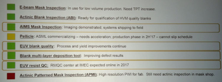
Intel and Samsung have talked about the prospects for EUV-lithography
![]()
|
xtreview is your : Video card - cpu - memory - Hard drive - power supply unit source |
|
|||
|
|
||||
 Recommended : Free unlimited image hosting with image editor
|
xtreview is your : Video card - cpu - memory - Hard drive - power supply unit source |
|
|
|
|
||
|
Xtreview Support  N-Post:xxxx Xtreview Support        |
INTEL AND SAMSUNG HAVE TALKED ABOUT THE PROSPECTS FOR EUV-LITHOGRAPHY |
| Please Feel Free to write any Comment; Thanks  |
Unofficially about Intels plans to release 300-series chipset (2017-09-08)
The European Court sent Intel case on abuses for reconsideration (2017-09-07)
The six-core processor Intel Coffee Lake lit up at a Chinese auction (2017-09-06)
Compact systems Intel NUC based on Coffee Lake will be released in the second quarter of 2018 (2017-09-05)
Ilon Mask believes that the third world war can begin artificial intelligence (2017-09-05)
The six-core processor Intel Coffee Lake has conquered the frequency of 5.0 GHz (2017-09-05)
Morningstar experts believe that Intel has a good potential in the field of artificial intelligence (2017-09-04)
The mention of Coffee Lake on the Intel site indicates the proximity of the announcement (2017-09-03)
Intel introduced Movidius Myriad X the visual center for robots became smarter (2017-08-29)
Intel stops supplying Xeon Phi 7200 Knights Landing coprocessors (2017-08-26)
Intel Core i7-8700K seen in the companys motherboard ASRock Z370 Pro4 (2017-08-26)
Former CFO Intel is preparing to leave the company (2017-08-25)
Expansion of 10-nm Intel processors range will be on 2018 (2017-08-24)
Leaks on the performance of Intel Core i3-8350K Coffee Lake (2017-08-24)
Six-core processors Intel Coffee Lake should be released in October (2017-08-22)
Analysts believe that the new processors from Intel and AMD will revive the PC market in the second half of the year (2017-08-22)
Atom C3000 processors registered in the Intel Price List (2017-08-19)
Intel and BMW gather around themselves new partners to develop robots (2017-08-17)
Details about the budget SoC Intel Gemini Lake (2017-08-15)
Intel introduced a new form factor for SSD servers line (2017-08-10)
![]()
To figure out your best laptops .Welcome to XTreview.com. Here u can find a complete computer hardware guide and laptop rating .More than 500 reviews of modern PC to understand the basic architecture


7600gt review
7600gt is the middle card range.
We already benchmarked this video card and found that ...

 geforce 8800gtx and 8800gts
  Xtreview software download Section
  AMD TURION 64 X2 REVIEW
  INTEL PENTIUM D 920 , INTEL PENTIUM D 930
  6800XT REVIEW
  computer hardware REVIEW
  INTEL CONROE CORE DUO 2 REVIEW VS AMD AM2
  INTEL PENTIUM D 805 INTEL D805
  Free desktop wallpaper
  online fighting game
  Xtreview price comparison center
 Lastest 15 Reviews


Rss Feeds
Last News
- The new version of GPU-Z finally kills the belief in the miracle of Vega transformation
- The motherboard manufacturer confirms the characteristics of the processors Coffee Lake
- We are looking for copper coolers on NVIDIA Volta computing accelerators
- Unofficially about Intels plans to release 300-series chipset
- The Japanese representation of AMD offered monetary compensation to the first buyers of Ryzen Threadripper
- This year will not be released more than 45 million motherboards
- TSMC denies the presentation of charges from the antimonopoly authorities
- Radeon RX Vega 64 at frequencies 1802-1000 MHz updated the record GPUPI 1B
- AMD itself would like to believe that mobile processors Ryzen have already been released
- AMD Vega 20 will find application in accelerating computations
- Pre-orders for new iPhone start next week
- Radeon RX Vega 57, 58 and 59: the wonders of transformation
- ASML starts commercial delivery of EUV-scanners
- The older Skylake processors with a free multiplier are removed from production
- Meizu will release Android-smartphone based on Helio P40
- AMD Bristol Ridge processors are also available in American retail
- The fate of Toshiba Memory can be solved to the next environment
- duo GeForce GTX 1080 Ti in GPUPI 1B at frequencies of 2480-10320 MHz
- New Kentsfield overclocking record up to 5204 MHz
- Lenovo released Android-smartphone K8

HALO 3 HALO 3 - Final Fight!

PREY Prey is something you don t often see anymore: a totally unigue shooter experience.

computer news computer parts review Old Forum Downloads New Forum Login Join Articles terms Hardware blog Sitemap Get Freebies


