- GeForce GTX 1080 Ti and Kaby Lake-X have distinguished themselves in Unigine Heaven Xtreme - GPU AMD Vega 10 design is a breakthrough for productivity growth - Samsung managed to become the largest manufacturer of semiconductor products - GPU AMD Vega 10 design is a breakthrough for productivity growth -
![]()
|
xtreview is your : Video card - cpu - memory - Hard drive - power supply unit source |
|
|
|
|
||
|
POSTER: computer news || GEFORCE GTX 1080 TI AND KABY LAKE-X HAVE DISTINGUISHED THEMSELVES IN UNIGINE HEAVEN XTREME |
DATE:2017-08-01 |
|
The American enthusiast Splave at the end of last week updated the absolute world record Unigine Heaven Xtreme, gaining 11 608.83 points DX11 with a video card GeForce GTX 1080 Ti and the central processor Intel Core i7-7740X. The latter was overclocked to 7.0 GHz with liquid nitrogen. 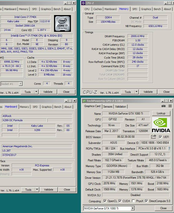 The video card ROG GeForce GTX 1080 Ti STRIX manufactured by Asus, as far as the available screenshot allows, was overclocked to 2190/12008 MHz using liquid nitrogen, or to even higher frequencies, which the author of the experiment was too shy to indicate in the HWBot database. But he explains that a reservoir for liquid nitrogen Der8auer Raptor was used. Thermal Grizzly was used everywhere, and the CPU was able to conquer the 7.1 GHz frequency. Select Rating :GeForce GTX 1080 Ti and Kaby Lake-X have distinguished themselves in Unigine Heaven Xtreme |
Add Comment ( 1 ) GEFORCE GTX 1080 TI AND KABY LAKE-X HAVE DISTINGUISHED THEMSELVES IN UNIGINE HEAVEN XTREME |
|
|
|
|
POSTER: computer news || GPU AMD VEGA 10 DESIGN IS A BREAKTHROUGH FOR PRODUCTIVITY GROWTH |
DATE:2017-08-01 |
|
The official announcement of video game cards on AMD Vega 10 architecture - Radeon RX Vega 56 and Radeon RX Vega 64 models - lifted the ban on publishing a number of details about the new graphics architecture. Due to leaks, some of the data was previously known, but now we have an official confirmation of all previously received unofficial information. So, the area of RX Vega graphics processor is 486 mm2, which is 112 mm2 less than the area of the Fiji graphics processor. At the same GPU Vega 10 has 12.5 billion transistors, while in the Fiji Fiji there are "only" 8.9 billion. It is not possible to explain the decrease in the labor GPU area . The previous processor was manufactured using a 28-nm process technology, while the GPU on the Vega 10 architecture is manufactured using the 14LPP process technology - this is the second generation of the 14-nm process technology. Reducing the geometric dimensions of the transistor has brought its effect - a smaller area was able to squeeze significantly more transistors (in the photo Vega 10 at the top, and Fiji at the bottom). 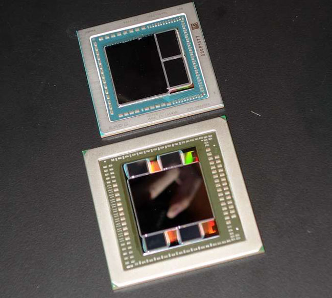 Another interesting thing is where did the "extra" budget from 3.9 billion transistors go, because the number of pipelines since the Fiji Fiji remained unchanged and equal to 4,096 units? As explained in AMD, the new architecture provides new levels of pipelines. Additional levels allow to "mask" the delay, which allow to significantly increase the speed of the new GPU. Thus, AMD Fiji graphics processors can operate at a frequency of up to 1.05 GHz, and GPUs on AMD Vega 10 are capable of operating at a frequency of up to 1.7 GHz. 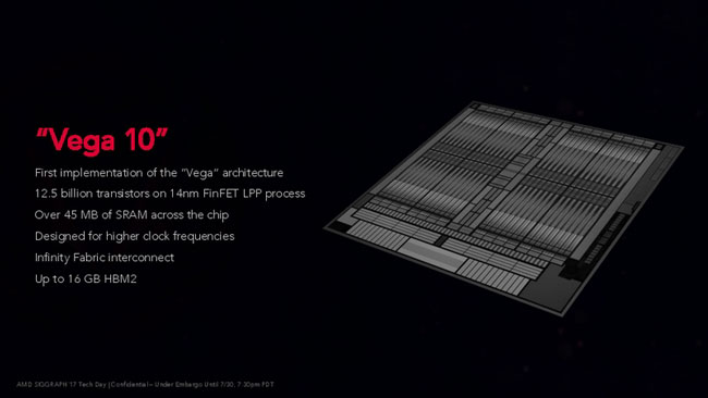 As we know, the transfer of production from technological standards of 28 nm to 14 nm gives the possibility of an increase in the clock frequency by approximately 30%. The GPU on the Vega 10 architecture from the transition to the 14LPP process technology was incremented by about 350 MHz. The increase of 400 MHz is the merit of AMD system architects. It is also officially confirmed that the ratio of FP64 units to FP32 units in the RX Vega GPU is 1/16, as in the case of other (previous) AMD video gaming and professional solutions of the previous generation. Such GPUs are not suitable for high-performance general purpose computing, but can be used in special niches where resources are required to accelerate FP16 and INT8 operations. First of all, it is a newfangled sphere with AI and deep machine learning. Finally, the RX Vega GPU can not use the ECC data integrity check feature, although the processor itself can work with HBM2 memory, which is initially armed with EEC support. In the processor for gaming adapters there is no necessary wiring. As for the use of HBM2 memory, there is one more interesting detail. According to our Japanese colleagues, gaming adapters carry two four-layer HBM2 chips, each of which has a capacity of 4 GB (the total amount of memory on the GPU RX Vega substrate is 8 GB). This means that each HBM2 stack in the RX Vega GPU consists of 8-Gbit memory chips. Potentially HBM2 stack can consist of 8 crystals. Select Rating :GPU AMD Vega 10 design is a breakthrough for productivity growth |
Add Comment ( 1 ) GPU AMD VEGA 10 DESIGN IS A BREAKTHROUGH FOR PRODUCTIVITY GROWTH |
|
|
|
|
POSTER: computer news || SAMSUNG MANAGED TO BECOME THE LARGEST MANUFACTURER OF SEMICONDUCTOR PRODUCTS |
DATE:2017-08-01 |
|
Experts have long predicted that the rise in prices for memory will allow Samsung Electronics in the second quarter to become the largest semiconductor manufacturer in the world in monetary terms. According to the EE Times website with reference to the estimates of IC Insights, in the first half of the year Samsung Electronics really managed to bypass Intel in terms of revenue, and become the largest player in the semiconductor market. Intel did not release the palm from its hands since 1992, but now IC Insights experts are sure that even the unstable nature of the memory market will not prevent Samsung Electronics from regularly heading this rating. The South Korean company's business can grow faster than the market, and Intel's likely figure will hardly exceed 5-6% per year, as the industry average. 
An excursion into the history of statistics in this direction allows us to conclude that Intel regularly increases its revenue, but Samsung Electronics is able to develop at a faster pace. In general, the participants in the "top ten" account for 58% of the semiconductor market revenue, so the trend towards consolidation and consolidation is clearly traced. Select Rating : Samsung managed to become the largest manufacturer of semiconductor products |
Add Comment ( 1 ) SAMSUNG MANAGED TO BECOME THE LARGEST MANUFACTURER OF SEMICONDUCTOR PRODUCTS |
|
|
|
|
POSTER: computer news || GPU AMD VEGA 10 DESIGN IS A BREAKTHROUGH FOR PRODUCTIVITY GROWTH |
DATE:2017-08-01 |
|
The official announcement of video game cards on AMD Vega 10 architecture - Radeon RX Vega 56 and Radeon RX Vega 64 models - lifted the ban on publishing a number of details about the new graphics architecture. Due to leaks, some of the data was previously known, but now we have an official confirmation of all previously received unofficial information. So, the area of RX Vega graphics processor is 486 mm2, which is 112 mm2 less than the area of the Fiji graphics processor. At the same GPU Vega 10 has 12.5 billion transistors, while in the Fiji Fiji there are "only" 8.9 billion. It is not possible to explain the decrease in the labor GPU area . The previous processor was manufactured using a 28-nm process technology, while the GPU on the Vega 10 architecture is manufactured using the 14LPP process technology - this is the second generation of the 14-nm process technology. Reducing the geometric dimensions of the transistor has brought its effect - a smaller area was able to squeeze significantly more transistors (in the photo Vega 10 at the top, and Fiji at the bottom).  Another interesting thing is where did the "extra" budget from 3.9 billion transistors go, because the number of pipelines since the Fiji Fiji remained unchanged and equal to 4,096 units? As explained in AMD, the new architecture provides new levels of pipelines. Additional levels allow to "mask" the delay, which allow to significantly increase the speed of the new GPU. Thus, AMD Fiji graphics processors can operate at a frequency of up to 1.05 GHz, and GPUs on AMD Vega 10 are capable of operating at a frequency of up to 1.7 GHz.  As we know, the transfer of production from technological standards of 28 nm to 14 nm gives the possibility of an increase in the clock frequency by approximately 30%. The GPU on the Vega 10 architecture from the transition to the 14LPP process technology was incremented by about 350 MHz. The increase of 400 MHz is the merit of AMD system architects. It is also officially confirmed that the ratio of FP64 units to FP32 units in the RX Vega GPU is 1/16, as in the case of other (previous) AMD video gaming and professional solutions of the previous generation. Such GPUs are not suitable for high-performance general purpose computing, but can be used in special niches where resources are required to accelerate FP16 and INT8 operations. First of all, it is a newfangled sphere with AI and deep machine learning. Finally, the RX Vega GPU can not use the ECC data integrity check feature, although the processor itself can work with HBM2 memory, which is initially armed with EEC support. In the processor for gaming adapters there is no necessary wiring. As for the use of HBM2 memory, there is one more interesting detail. According to our Japanese colleagues, gaming adapters carry two four-layer HBM2 chips, each of which has a capacity of 4 GB (the total amount of memory on the GPU RX Vega substrate is 8 GB). This means that each HBM2 stack in the RX Vega GPU consists of 8-Gbit memory chips. Potentially HBM2 stack can consist of 8 crystals. Select Rating :GPU AMD Vega 10 design is a breakthrough for productivity growth |
Add Comment ( 1 ) GPU AMD VEGA 10 DESIGN IS A BREAKTHROUGH FOR PRODUCTIVITY GROWTH |
|
|
|
|
xtreview is your : Video card - cpu - memory - Hard drive - power supply unit source |
|
|
|
|
||
![]()
To figure out your best laptops .Welcome to XTreview.com. Here u can find a complete computer hardware guide and laptop rating .More than 500 reviews of modern PC to understand the basic architecture


7600gt review
7600gt is the middle card range.
We already benchmarked this video card and found that ...

 geforce 8800gtx and 8800gts
  Xtreview software download Section
  AMD TURION 64 X2 REVIEW
  INTEL PENTIUM D 920 , INTEL PENTIUM D 930
  6800XT REVIEW
  computer hardware REVIEW
  INTEL CONROE CORE DUO 2 REVIEW VS AMD AM2
  INTEL PENTIUM D 805 INTEL D805
  Free desktop wallpaper
  online fighting game
  Xtreview price comparison center

- 233 - E8600 vs q9400 which is better dual or quad core
Date : 2008-11-21
- 216 - Intel core 2 duo e6550 review and overclocking
Date : 2007-08-03
- 212 - Intel core 2 extreme qx6850 and core 2 duo e6850 review benchmark and overclocking
Date : 2007-07-16
- 205 - Amd athlon x2 be review , overclocking and energy consumption test
Date : 2007-06-05
- 229 - Radeon hd 4670 vs geforce 9500 gt vs geforce 9800 gt vs hd 4850 overclock benchmark and review
Date : 2008-10-10
- 228 - Crossfire hd 4870 x2 vs crossfire hd 4870 review and benchamrk
Date : 2008-09-26
- 226 - Amd radeon hd 4870 x2 2x1gb xtreview exclusive review
Date : 2008-07-14
- 220 - Nvidia 9600 gt review and benchmark
Date : 2008-02-27
- 131 - 500 to 750 gig hdd round up : maxtor wd seagate hitachi
Date : 2006-07-10
- 65 - Raptor x hdd western digital review overview : pcmark - benchmark - test
Date : 2006-05-06
- 193 - Asus s6fm-1p039e vs sony vaio vgn-g11xn/b vs lenovo 3000 v100 review and benchmark
Date : 2007-05-11
- 172 - Apple imac 20 inch - intel core 2 duo review
Date : 2007-01-26
- 102 - Toshiba tecra a6-s513 review notebook performance benchmark
Date : 2006-06-09
- 101 - Sony vgn-fj1sr review notebook performance benchmark
Date : 2006-06-09
SnagIt v.9.1.22009-04-24
Daemon Tool v.4.30.42009-04-24
WinSCP v.4.1.92009-04-24
Vista Codec Package v.5.2.02009-04-24
Vista Codec x64 Components v.1.8.12009-04-24
Anti-keylogger v.9.2.12009-04-24
Portable Firefox v.3.0.92009-04-24
AVG Internet Security v.8.5.322a14952009-04-24
Universal Viewver v.4.0.02009-04-24
Wise Disk Cleaner v.4.242009-04-24
FeedDemon v.3.0.0.16 Beta2009-04-24
SiSoft Sandra 2009 SP2 (2009.5.15.96)2009-04-24
Atheros AR5xxx Driver v.7.7.0.2332009-04-24
Bios update for 24 April2009-04-24
AIMP Classic v.2.60 Build 466 Beta 12009-04-23
SpeedFan v.4.382009-04-23
- The new version of GPU-Z finally kills the belief in the miracle of Vega transformation
- The motherboard manufacturer confirms the characteristics of the processors Coffee Lake
- We are looking for copper coolers on NVIDIA Volta computing accelerators
- Unofficially about Intels plans to release 300-series chipset
- The Japanese representation of AMD offered monetary compensation to the first buyers of Ryzen Threadripper
- This year will not be released more than 45 million motherboards
- TSMC denies the presentation of charges from the antimonopoly authorities
- Radeon RX Vega 64 at frequencies 1802-1000 MHz updated the record GPUPI 1B
- AMD itself would like to believe that mobile processors Ryzen have already been released
- AMD Vega 20 will find application in accelerating computations
- Pre-orders for new iPhone start next week
- Radeon RX Vega 57, 58 and 59: the wonders of transformation
- ASML starts commercial delivery of EUV-scanners
- The older Skylake processors with a free multiplier are removed from production
- Meizu will release Android-smartphone based on Helio P40
- AMD Bristol Ridge processors are also available in American retail
- The fate of Toshiba Memory can be solved to the next environment
- duo GeForce GTX 1080 Ti in GPUPI 1B at frequencies of 2480-10320 MHz
- New Kentsfield overclocking record up to 5204 MHz
- Lenovo released Android-smartphone K8
Affiliates


computer news computer parts review OLD Forum Downloads New Forum Login Join Articles terms Hardware blog Sitemap myspace proxy Get Freebies


