OOPS! You forgot to upload swfobject.js ! You must upload this file for your form to work.
Intel IDF 2009 22 nm
![]()
|
xtreview is your : Video card - cpu - memory - Hard drive - power supply unit source |
|
|||
|
|
||||
 Recommended : Free unlimited image hosting with image editor
|
POSTER: computer news || INTEL IDF 2009 22 NM |
DATE:2009-09-23 |
|
|
The Director-General and Intel corporation President (Paul otellini) demonstrated the first microcircuits models , prepared according to 22- nm technological process standards.  Mastering ever thinner technological standards, Intel continues to prove the validity of Moore's law.  In the chips, announced two years after the mastery of 32- nm technological process, the third generation of Hi- K technology with the metallic lock is realized.  New development sequential time confirmed that Moore's law satisfactorily stepped over the conditional boundary, beyond which, in the opinion experts, the semiconductor industry must encounter insoluble problems. 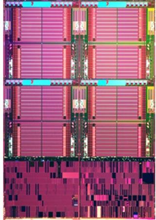 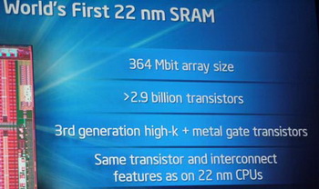 Only after the achievement of success with these products on the new technology , Intel will switch over the release of new generation processors . 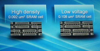 Now Intel works at the adoption of 22 nm standards in the mass production of microcircuits . 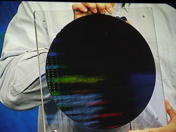 The test microcircuits, released with 22 nm standards are SRAM memory and logical modules. SRAM- cells with size of 0,108 and 0,092 sq. m function in the composition of array on 364 ml bits. 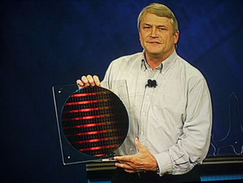 Cell sq. m am optimized by the area of 0,108 for work in the low-voltage region, while cell with the area 0,092 sq. m is the smallest known today cells SRAM. 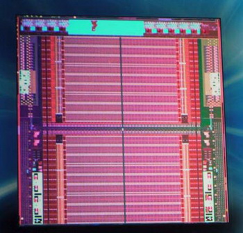 For the achievement of this result Intel uses lithograph with wavelength 193 nm. Related Products : | ||
|
|
||
|
xtreview is your : Video card - cpu - memory - Hard drive - power supply unit source |
|
|
|
|
||
|
Xtreview Support  N-Post:xxxx Xtreview Support        |
INTEL IDF 2009 22 NM |
| Please Feel Free to write any Comment; Thanks  |
Intel has canceled annual forums IDF (2017-04-18)
Photos 140 GB SSD Intel Optane IDF 2016 (2016-08-28)
In Shenzhen at IDF 2016, Intel showed the work of SSD memory 3D XPoint (2016-04-16)
At the next IDF session ntel will focus on the Internet of Things (2016-03-28)
At IDF 2015 was featured a system with 14-nm processors Xeon Phi (2015-08-21)
At IDF 2015 a pair of external graphics cards for laptops (2015-08-20)
IDF 2015 More information about the architecture of Intel Skylake (2015-08-19)
IDF 2015 Sample laptop-tablet with a second screen E Ink (2015-04-14)
At IDF 2015, Intel showed convertible notebook without power connectors (2015-04-12)
IDF 2015 Intel - lord spider (2015-04-09)
IDF 2014 A few words about the single-chip processors Xeon D-DE (2014-09-14)
Important slides from the first day of IDF 2014 (2014-09-11)
IDF 2014 Intel demonstrated a laptop and desktop processors Skylake (2014-09-10)
Intel will show a 14-nm processors at IDF in September (2014-07-11)
At IDF 2014 Intel again mentioned Braswell and Broadwell (2014-04-03)
IDF 2014 Intel has demonstrated USB-connector Type-C (2014-04-03)
Photos of Broadwell CPUs IDF 2013 (2013-09-13)
G.SKill IDF TPU (2013-09-13)
IDF 2013 demonstration of DDR4 memory (2013-09-12)
IDF 2013 Bay Trail (2013-09-12)
![]()
To figure out your best laptops .Welcome to XTreview.com. Here u can find a complete computer hardware guide and laptop rating .More than 500 reviews of modern PC to understand the basic architecture


7600gt review
7600gt is the middle card range.
We already benchmarked this video card and found that ...

 geforce 8800gtx and 8800gts
  Xtreview software download Section
  AMD TURION 64 X2 REVIEW
  INTEL PENTIUM D 920 , INTEL PENTIUM D 930
  6800XT REVIEW
  computer hardware REVIEW
  INTEL CONROE CORE DUO 2 REVIEW VS AMD AM2
  INTEL PENTIUM D 805 INTEL D805
  Free desktop wallpaper
  online fighting game
  Xtreview price comparison center
 Lastest 15 Reviews


Rss Feeds
Last News
- The new version of GPU-Z finally kills the belief in the miracle of Vega transformation
- The motherboard manufacturer confirms the characteristics of the processors Coffee Lake
- We are looking for copper coolers on NVIDIA Volta computing accelerators
- Unofficially about Intels plans to release 300-series chipset
- The Japanese representation of AMD offered monetary compensation to the first buyers of Ryzen Threadripper
- This year will not be released more than 45 million motherboards
- TSMC denies the presentation of charges from the antimonopoly authorities
- Radeon RX Vega 64 at frequencies 1802-1000 MHz updated the record GPUPI 1B
- AMD itself would like to believe that mobile processors Ryzen have already been released
- AMD Vega 20 will find application in accelerating computations
- Pre-orders for new iPhone start next week
- Radeon RX Vega 57, 58 and 59: the wonders of transformation
- ASML starts commercial delivery of EUV-scanners
- The older Skylake processors with a free multiplier are removed from production
- Meizu will release Android-smartphone based on Helio P40
- AMD Bristol Ridge processors are also available in American retail
- The fate of Toshiba Memory can be solved to the next environment
- duo GeForce GTX 1080 Ti in GPUPI 1B at frequencies of 2480-10320 MHz
- New Kentsfield overclocking record up to 5204 MHz
- Lenovo released Android-smartphone K8

HALO 3 HALO 3 - Final Fight!

PREY Prey is something you don t often see anymore: a totally unigue shooter experience.

computer news computer parts review Old Forum Downloads New Forum Login Join Articles terms Hardware blog Sitemap Get Freebies


