Nvidia GF100 architecture in detail
![]()
|
xtreview is your : Video card - cpu - memory - Hard drive - power supply unit source |
|
|||
|
|
||||

 Recommended : Free unlimited image hosting with image editor
|
POSTER: computer news || NVIDIA GF100 ARCHITECTURE IN DETAIL |
DATE:2010-01-20 |
|
|
Today appeared new information about Fermi and GF100 . The new architecture has many revolutionary and evolutionary changes, let us examine them based on the example of GF100. Chip will consist of the following global blocks:
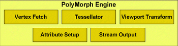
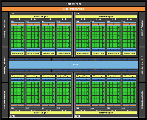 The PCI express , image controllers and the block gigaThread engine do not need an idea, but here let us examine in more detail. We start from Graphics processing cluster. Actually, this is independent graphic processor, which in GF100 are four pieces, which removes a whole series of limitations and enlarges the bottlenecks of graphic conveyor. On NVIDIA statements , Fermi was developed taking into account all special features Of directX 11 and basic difference from the previous architecture appears an increase of geometric productivity by several times. Each Graphics processing cluster consists of one block (not to confuse with ROP) and four SM (Streaming multiprocessors). 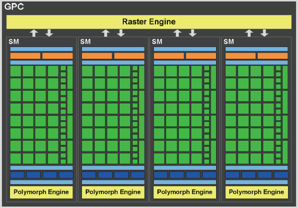
Each SM, in turn, it consists of:
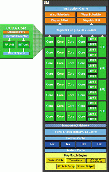 Let us talk in greater detail on the latter. This block answers for five stages of graphic conveyor - sample apexes, conversion in the screen coordinates, installation of an attributes and thread conclusions.
The first important conclusion of GF100 does not have the united chosen block of tessellation as Cypress, but each GPC has four similar blocks, which allow to a considerable degree execute in parallel this operation. Now the question is one large block of tessellation (AMD) or sixteen small (NVIDIA) is better? Answer to this question is demonstrated by tests NVIDIA results , where the Nvidia solution goes around Radeon HD 5870 2-6 times. 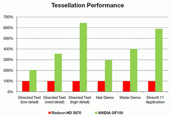 Of course similar superiority relates to the synthetic and semisynthetic tests of tessellation, but not general productivity of chip. With the comparison Of radeon HD 5870 and GF100 in the popular test unigine heaven the latter demonstrates superiority over rival approximately by 1.6 times. 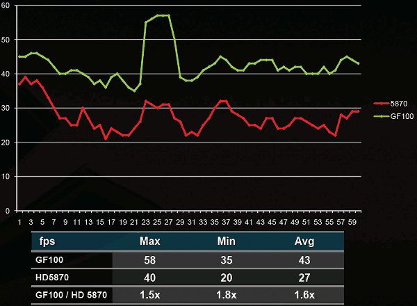 In the popular game far cry 2 future NVIDIA card demonstrates analogous indices : it was one and a half times faster than elder one chip solution from AMD. However, in 3DMark vantage, using extreme setting, GF100 is faster than Radeon HF 5870 approximately by 80%. All in all, according to the first tests results it is possible to note that GF100 is considerably faster than one chip AMD card card, it is actually compared with the two-chip solution radeon HD 5970. The total number of sample and textures filtering blocks is only 64 pieces, which is less than in Cypress and GT200 (80 pieces). NVIDIA asserts that they succeeded in considerably increasing the effectiveness of their work, which is 40-60% superior to GT200. 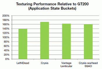 Some independent specialists even assume that TMU now operate at the shader frequency . By the way, about the frequencies. Solutions on base Of g80 had two independent frequencies : core and shader domain. Moreover, the second was always more than double of the first . In Fermi , as the fundamental chip frequency now is considered the shader frequency , which in GF100 is within the limits 1400-1500 MHz, and the remaining blocks frequency is now rigid through reducing coefficient 1/2. Last component in fermi architecture is the memory controllers , ROP blocks cache second level. The general cache in the second level (768 KB) is broken in six blocks on 128 KB, which communicate directly with the memory controller and ROP blocks. The memory controllers of GF100 support GDDR- 5 memories and have a 384 bits bus , which increase the memory capacity more than one and a half times in comparison with GT200. The scanning operation's blocks (ROP) also underwent changes in comparison with GT200. Their number per channel is doubled (8 pieces to each memory controller , in all in GF100 there are 48 pieces, in GT200 32 pieces), and effectiveness is increased, which allow the G100 to anticipate GeForce GTX 285, with the use of 8x smoothing more than twice. 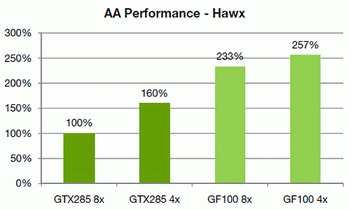 NVIDIA made immediately two interesting update : considerably improve architecture for GPGPU and simultaneously produce a number of revolutionary and evolutionary changes for an increase of productivity in 3d applications. At the conclusion, we can share fresh rumors relative to new card from NVIDIA. Nvidia plan to release two solutions, with the assumed names GeForce GTX 380 and GeForce GTX 360. The first product will be high end , compete with Radeon HD 5970, energy consumption of approximately 280 W and cost of approximately $500-550. The low-end solution will have fewer numbers of blocks and a little anticipate Radeon HD 5870 ($399). Supposedly, the number of its actuating elements will be reduced doubly, in comparison with GF100 and it will consist of two blocks GPC. Clock frequencies can be scarcely higher, then in GF100, which will allow to demonstrate productivity at the level 50-55% in comparison with high end card. It is assumed that GF104 will appear simultaneously with GF100 or in the nearest time . 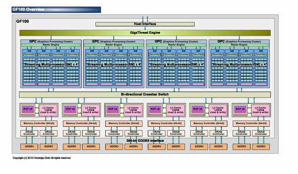 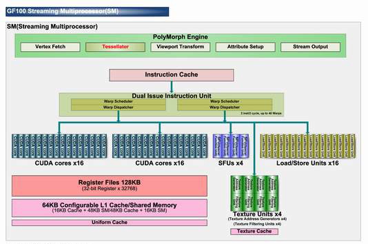 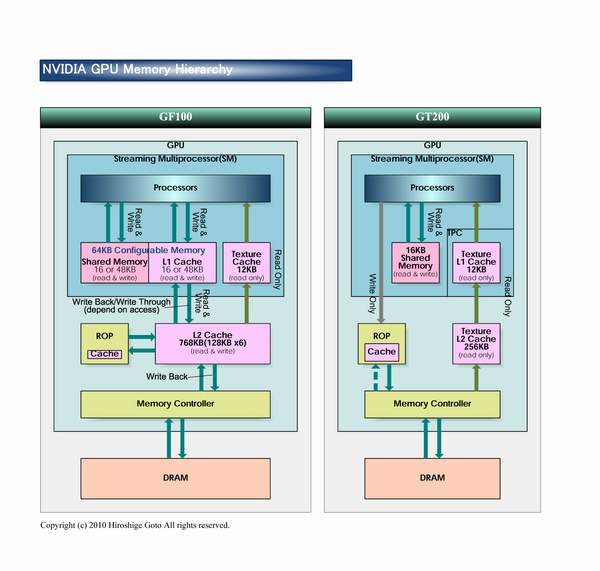 Related Products : | ||
|
|
||

|
xtreview is your : Video card - cpu - memory - Hard drive - power supply unit source |
|
|
|
|
||
|
Xtreview Support  N-Post:xxxx Xtreview Support  |
NVIDIA GF100 ARCHITECTURE IN DETAIL |
| Please Feel Free to write any Comment; Thanks  |
GeForce GTX 460 with 1 Gb memory will use GF100 chip (2010-07-08)
NVIDIA will speak only about GF100 at the conference Of hot chips (2010-06-24)
GF100 for notebooks soon (2010-04-22)
Nvidia refute rumor about low level of suitable GF100 chip (2010-04-13)
CoolIT Omni ALC GF100 (2010-03-27)
AMD does not fear GF100 (2010-03-25)
NVIDIA representatives deny GF100 price rumors (2010-03-01)
NVIDIA GF100 performance and price (2010-03-01)
GF100 estimated price (2010-01-24)
GF100 sale date (2010-01-24)
Nvidia GF100 architecture in detail (2010-01-20)
Nvidia Givne away a GF100 (2010-01-12)
GF100 specific announcement periods (2010-01-12)
GF100 3- way SLI performance (2010-01-08)
GF100 fermi demonstrated (2010-01-07)
GF100 in CES 2010 (2010-01-04)
GF100 will decode volumetric blu-ray video and support 32x- smoothing (2009-12-29)
GF100 will support voltage increase (2009-12-19)
GF100 in SLI (2009-12-08)
NVIDIA card GF100 (2009-11-21)
![]()
To figure out your best laptops .Welcome to XTreview.com. Here u can find a complete computer hardware guide and laptop rating .More than 500 reviews of modern PC to understand the basic architecture


7600gt review
7600gt is the middle card range.
We already benchmarked this video card and found that ...
 geforce 8800gtx and 8800gts Xtreview software download Section AMD TURION 64 X2 REVIEW INTEL PENTIUM D 920 , INTEL PENTIUM D 930 6800XT REVIEW computer hardware REVIEW INTEL CONROE CORE DUO 2 REVIEW VS AMD AM2 INTEL PENTIUM D 805 INTEL D805 Free desktop wallpaper online fighting game Xtreview price comparison center
Rss Feeds

- The new version of GPU-Z finally kills the belief in the miracle of Vega transformation
- The motherboard manufacturer confirms the characteristics of the processors Coffee Lake
- We are looking for copper coolers on NVIDIA Volta computing accelerators
- Unofficially about Intels plans to release 300-series chipset
- The Japanese representation of AMD offered monetary compensation to the first buyers of Ryzen Threadripper
- This year will not be released more than 45 million motherboards
- TSMC denies the presentation of charges from the antimonopoly authorities
- Radeon RX Vega 64 at frequencies 1802-1000 MHz updated the record GPUPI 1B
- AMD itself would like to believe that mobile processors Ryzen have already been released
- AMD Vega 20 will find application in accelerating computations
- Pre-orders for new iPhone start next week
- Radeon RX Vega 57, 58 and 59: the wonders of transformation
- ASML starts commercial delivery of EUV-scanners
- The older Skylake processors with a free multiplier are removed from production
- Meizu will release Android-smartphone based on Helio P40
- AMD Bristol Ridge processors are also available in American retail
- The fate of Toshiba Memory can be solved to the next environment
- duo GeForce GTX 1080 Ti in GPUPI 1B at frequencies of 2480-10320 MHz
- New Kentsfield overclocking record up to 5204 MHz
- Lenovo released Android-smartphone K8


computer news computer parts review Old Forum Downloads New Forum Login Join Articles terms Hardware blog Sitemap Get Freebies