OOPS! You forgot to upload swfobject.js ! You must upload this file for your form to work.
GlobalFoundries demonstrated working 20 nm solutions using cross-connections
![]()
|
xtreview is your : Video card - cpu - memory - Hard drive - power supply unit source |
|
|||
|
|
||||
 Recommended : Free unlimited image hosting with image editor
|
POSTER: computer news || GLOBALFOUNDRIES DEMONSTRATED WORKING 20 NM SOLUTIONS USING CROSS-CONNECTIONS |
DATE:2013-04-03 |
|
|
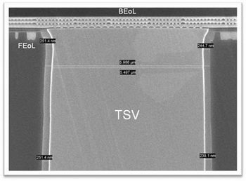
TSVs is relatively new technology - , which involves the creation of vertical wires (metalized channels) between upper and lower crystals in the stack. Feedthrough narrow footprint chip to chip area and save consumption by drastically reducing the lengths of connections. In addition, for short wire significantly increases the rate of exchange. Yesterday about the latest success in the field of practical implementation of TSVs-compounds reported GlobalFoundries company. According to an official press release from the manufacturer, the American company's factory - Fab 8 - managed to get the first plate with work items of 20 nm using a vertical cross-connections. This complex process is implemented for the so-called process technology 20nm-LPM. It is not suitable for the production of the CPU, but it is suitable for mobile applications, to produce solutions for the consumer electronics and production controllers. Hopefully, the manufacturer adopts TSVs for something better.  For the release of 3-D semiconductors with through connections GlobalFoundries uses so-called via-middle process. The approach is to fill the holes for copper plating on the penultimate stage of the proceedings, when the whole set is made of crystals, and the package has not yet been carried out. This avoids problems with the two-layer metal (copper) connections at the time of manufacture of each layer, where the operating temperatures for copper are extremely high. The first commercial solutions using TSVs-compounds the company will not release until 2015.  JEDEC is close to the assertion of the memory interface, as Wide IO (up to 12 Gbit / s). One package contains a memory interface Wide IO can be used up to four crystals with conventional wire . Release this memory is easier than in a stacking configuration, so Texas Instruments and STMicroelectronics company, for instance, abandoned the idea of working with TSVs. Finally, the packing stack memory and other crystals can only deal with companies that specialize in this activity type - Amkor, ASE and others. It is clear that it will not make the final chip cheaper. All because of the complexity of multi-dimensional packaging of chips when you need to separate each crystal from the time the carrier substrate and then link them together. Related Products : | ||
|
|
||
|
xtreview is your : Video card - cpu - memory - Hard drive - power supply unit source |
|
|
|
|
||
|
Xtreview Support  N-Post:xxxx Xtreview Support        |
GLOBALFOUNDRIES DEMONSTRATED WORKING 20 NM SOLUTIONS USING CROSS-CONNECTIONS |
| Please Feel Free to write any Comment; Thanks  |
HTC U 11 on Snapdragon 835 demonstrated a promising result in GeekBench (2017-04-30)
MSI demonstrated automatic overclocking Kaby Lake up to 5.2 GHz (2017-01-18)
AMD demonstrated the possibility Ryzen processor Zen (2016-12-14)
Console Nintendo Switch demonstrated live (2016-12-10)
AMD has already demonstrated new products to a narrow circle of people (2016-12-09)
Intel demonstrated Broadwell-EP processors with built-in dies Altera (2016-11-17)
NVIDIA demonstrated a mobile Quadro on GPU Pascal (2016-07-27)
Boston Dynamics has demonstrated the possibility of domestic four-legged robot (2016-06-24)
At Computex 2016 demonstrated a motherboard with integrated GeForce GTX 1070 (2016-06-05)
At Computex 2016, AMD demonstrated the processor Summit Ridge Zen (2016-06-01)
AMD demonstrated the possibility of Polaris 10 in Doom QuadHD (2016-05-30)
Working NVIDIA Pascal samples can be demonstrated in early April (2016-02-24)
dual Fiji system was demonstrated on Los Angeles (2016-01-25)
Google demonstrated a robot-car sled (2015-12-23)
NEC demonstrated drones detection system (2015-10-09)
Quad GeForce GTX 980 Ti once again demonstrated the power of water cooling in Catzilla (2015-09-15)
At Computex 2015 graphics card AMD Fury demonstrated only partners to the company (2015-06-06)
AMD demonstrated its FreeSync via HDMI (2015-06-06)
Intel demonstrated a sample tablet on Skylake processor (2015-06-03)
OCZ announced new SSD-drives Trion 100 on TLC NAND memory and demonstrated NVMe SSD (2015-06-02)
![]()
To figure out your best laptops .Welcome to XTreview.com. Here u can find a complete computer hardware guide and laptop rating .More than 500 reviews of modern PC to understand the basic architecture


7600gt review
7600gt is the middle card range.
We already benchmarked this video card and found that ...

 geforce 8800gtx and 8800gts
  Xtreview software download Section
  AMD TURION 64 X2 REVIEW
  INTEL PENTIUM D 920 , INTEL PENTIUM D 930
  6800XT REVIEW
  computer hardware REVIEW
  INTEL CONROE CORE DUO 2 REVIEW VS AMD AM2
  INTEL PENTIUM D 805 INTEL D805
  Free desktop wallpaper
  online fighting game
  Xtreview price comparison center
 Lastest 15 Reviews


Rss Feeds
Last News
- The new version of GPU-Z finally kills the belief in the miracle of Vega transformation
- The motherboard manufacturer confirms the characteristics of the processors Coffee Lake
- We are looking for copper coolers on NVIDIA Volta computing accelerators
- Unofficially about Intels plans to release 300-series chipset
- The Japanese representation of AMD offered monetary compensation to the first buyers of Ryzen Threadripper
- This year will not be released more than 45 million motherboards
- TSMC denies the presentation of charges from the antimonopoly authorities
- Radeon RX Vega 64 at frequencies 1802-1000 MHz updated the record GPUPI 1B
- AMD itself would like to believe that mobile processors Ryzen have already been released
- AMD Vega 20 will find application in accelerating computations
- Pre-orders for new iPhone start next week
- Radeon RX Vega 57, 58 and 59: the wonders of transformation
- ASML starts commercial delivery of EUV-scanners
- The older Skylake processors with a free multiplier are removed from production
- Meizu will release Android-smartphone based on Helio P40
- AMD Bristol Ridge processors are also available in American retail
- The fate of Toshiba Memory can be solved to the next environment
- duo GeForce GTX 1080 Ti in GPUPI 1B at frequencies of 2480-10320 MHz
- New Kentsfield overclocking record up to 5204 MHz
- Lenovo released Android-smartphone K8

HALO 3 HALO 3 - Final Fight!

PREY Prey is something you don t often see anymore: a totally unigue shooter experience.

computer news computer parts review Old Forum Downloads New Forum Login Join Articles terms Hardware blog Sitemap Get Freebies


