The traditional technology of NAND flash memory will last for two generations of process technology

|
xtreview is your : Video card - cpu - memory - Hard drive - power supply unit source |
|
|||
|
|
||||


 Recommended : Free unlimited image hosting with image editor
|
POSTER: computer news || THE TRADITIONAL TECHNOLOGY OF NAND FLASH MEMORY WILL LAST FOR TWO GENERATIONS OF PROCESS TECHNOLOGY |
DATE:2013-05-26 |
|
|
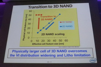
During the event, Imec Technology, held this week in Belgium, IM Flash Technologies company, a joint venture between Intel and Micron Technologies, has shed light on the development of plans for the three-dimensional layout of chip technology in the production of flash memory. The industry is now beginning to shift from planar placement of NAND memory cells to layout with vertical integration of transistors. This approach allows us to form a cell capable of storing multiple bits of information due to the presence of the vertical channel and a gate corresponding to different stress levels . The leader of the company direction was Toshiba, which has developed technology p-BiCS (pipe-shaped Bit Cost Scalable). Late last year, the Japanese manufacturer announced the creation of 16-layer memory that uses a vertical channel with a diameter of 50 nm. According to IM Flash Technologies, limit reduction of traditional flash memory is already close, but the existing technology will suffice for another two-generation technology standards - 15 and 10 nanometers - . The development of three-dimensional layout unfold on stage, corresponding to 15 nm. Interestingly, the 16 layers, as calculated by IM Flash Technologies, is not enough to make the venture economically viable. At least to 32, and more preferably - 64 layers. | ||
|
|
||
|
xtreview is your : Video card - cpu - memory - Hard drive - power supply unit source |
|
|
|
|
||
|
Xtreview Support  N-Post:xxxx Xtreview Support  |
THE TRADITIONAL TECHNOLOGY OF NAND FLASH MEMORY WILL LAST FOR TWO GENERATIONS OF PROCESS TECHNOLOGY |
| Please Feel Free to write any Comment; Thanks  |
SMARTPHONES OF THE FUTURE CAN work WITHOUT TRADITIONAL BATTERIES (2017-08-14)
Intel life outside the traditional CMOS process technology (2017-04-04)
The first iPhone without the traditional Home button will appear not earlier than 2017 (2015-06-23)
Montblanc starts selling smart wristbands for the traditional watch in June (2015-05-22)
This year, Samsung will refrain from raising wages to traditional employees (2015-02-27)
Demand for traditional hard drives will decline faster than the demand for PC (2015-01-29)
ASUS and MSI may affect the traditional suppliers of desktop computers (2014-08-06)
The traditional technology of NAND flash memory will last for two generations of process technology (2013-05-26)
This year, the traditional PC market expects decline in sales (2012-07-03)
Samsung say that the traditional model of chips production is outdated (2012-06-27)
Light peak first generation with traditional copper conductors (2010-12-10)

To figure out your best laptops .Welcome to XTreview.com. Here u can find a complete computer hardware guide and laptop rating .More than 500 reviews of modern PC to understand the basic architecture


7600gt review
7600gt is the middle card range.
We already benchmarked this video card and found that ...
 geforce 8800gtx and 8800gts Xtreview software download Section AMD TURION 64 X2 REVIEW INTEL PENTIUM D 920 , INTEL PENTIUM D 930 6800XT REVIEW computer hardware REVIEW INTEL CONROE CORE DUO 2 REVIEW VS AMD AM2 INTEL PENTIUM D 805 INTEL D805 Free desktop wallpaper online fighting game Xtreview price comparison center
Rss Feeds


- The new version of GPU-Z finally kills the belief in the miracle of Vega transformation
- The motherboard manufacturer confirms the characteristics of the processors Coffee Lake
- We are looking for copper coolers on NVIDIA Volta computing accelerators
- Unofficially about Intels plans to release 300-series chipset
- The Japanese representation of AMD offered monetary compensation to the first buyers of Ryzen Threadripper
- This year will not be released more than 45 million motherboards
- TSMC denies the presentation of charges from the antimonopoly authorities
- Radeon RX Vega 64 at frequencies 1802-1000 MHz updated the record GPUPI 1B
- AMD itself would like to believe that mobile processors Ryzen have already been released
- AMD Vega 20 will find application in accelerating computations
- Pre-orders for new iPhone start next week
- Radeon RX Vega 57, 58 and 59: the wonders of transformation
- ASML starts commercial delivery of EUV-scanners
- The older Skylake processors with a free multiplier are removed from production
- Meizu will release Android-smartphone based on Helio P40
- AMD Bristol Ridge processors are also available in American retail
- The fate of Toshiba Memory can be solved to the next environment
- duo GeForce GTX 1080 Ti in GPUPI 1B at frequencies of 2480-10320 MHz
- New Kentsfield overclocking record up to 5204 MHz
- Lenovo released Android-smartphone K8












computer news computer parts review Old Forum Downloads New Forum Login Join Articles terms Hardware blog Sitemap Get Freebies


