OOPS! You forgot to upload swfobject.js ! You must upload this file for your form to work.
Intel company released EDRAM chip from an array of FinFET transistors
![]()
|
xtreview is your : Video card - cpu - memory - Hard drive - power supply unit source |
|
|||
|
|
||||
 Recommended : Free unlimited image hosting with image editor
|
POSTER: computer news || INTEL COMPANY RELEASED EDRAM CHIP FROM AN ARRAY OF FINFET TRANSISTORS |
DATE:2013-06-18 |
|
|
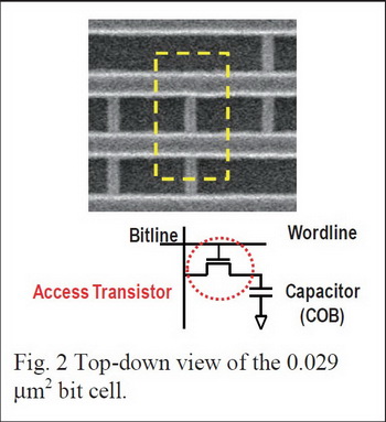
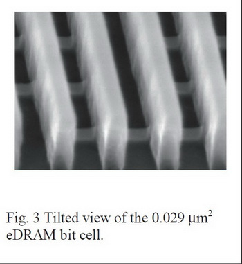
Intel release its own eDRAM module. As we learned from the report of the company for its manufacture will be used the same 22-nm HKMG-process as for the production of processors (the differences are in the materials for the insulator and gate). The multilayer structure of crystals with nine metal layers allow to arrange one of the layers to maintain the charge capacity - the insulator layer is surrounded by two layers of metal foil. Managing eDRAM memory cell transistor is the same in structure FinFET-transistor as the active element in the logic of Haswell. Intel does not have to invent anything - the decision came an elegant and simple in its own way. Thus in the memory transistor can operate at a voltage that in 0.75-1 significantly lower power common memory.  EDRAM cell area at the 22-nm process technology, reduced to 0,029 square meters. um. SRAM cell area in the same process technology, is 0,092 square meters. - is three times more. That is eDRAM is much denser and energy-efficient usual cache.  This kind of technology was made by IBM. The cell eDRAM IBM slightly smaller area than the cell eDRAM Intel and is 0,026 square meters. um. This is due to the fact that the cells have an in-depth capacitors - they are smaller in size in the section. At the same time, according to Intel, they have the same density - about 17.5 Mbits / m. mm. Intel company has another distinct advantage. Its eDRAM is already in mass production. Related Products : | ||
|
|
||
|
xtreview is your : Video card - cpu - memory - Hard drive - power supply unit source |
|
|
|
|
||
|
Xtreview Support  N-Post:xxxx Xtreview Support        |
INTEL COMPANY RELEASED EDRAM CHIP FROM AN ARRAY OF FINFET TRANSISTORS |
| Please Feel Free to write any Comment; Thanks  |
Analysts at Bernstein believe that Apples augmented reality glasses could lead the company to success (2017-08-28)
Intel Core i7-8700K seen in the companys motherboard ASRock Z370 Pro4 (2017-08-26)
Former CFO Intel is preparing to leave the company (2017-08-25)
The last quarter for the company Sony was successful (2017-08-03)
Veteran processor developer leaves Intel company (2017-07-22)
A week later, Toshiba will determine the buyer of the companys semiconductor business (2017-06-08)
AMD representatives could not support the share price of the company (2017-05-18)
British company told about self-charging battery (2017-04-27)
The first images of Radeon RX 500 video cards from Sapphire company (2017-04-12)
Chinese company SMIC is determined to master the production of 7-nm semiconductor products (2017-03-15)
GM plans to create the largest auto taxi cab company in the next year (2017-02-18)
Shares of Samsung are getting cheaper against the background of rumors about the impending arrest of the head of the company (2017-02-15)
The head of Valve, said the company is working on a singles-based Source 2 (2017-01-18)
Apple recognized as the most innovative company in the world (2017-01-15)
For investor confidence in the strength of Vega NVIDIA company had to pay a decrease in the share price (2016-12-30)
Watch out for eyes Facebook bought the company for Oculus Eye Tribe (2016-12-30)
TDK buys developer of motion sensor company InvenSense (2016-12-22)
Robocar project was allocated to the company Google Waymo (2016-12-14)
AMD Zen is very competitive, according to the head of the company (2016-12-01)
This week, Samsung Electronics is to decide whether the company should be split (2016-11-28)
![]()
To figure out your best laptops .Welcome to XTreview.com. Here u can find a complete computer hardware guide and laptop rating .More than 500 reviews of modern PC to understand the basic architecture


7600gt review
7600gt is the middle card range.
We already benchmarked this video card and found that ...

 geforce 8800gtx and 8800gts
  Xtreview software download Section
  AMD TURION 64 X2 REVIEW
  INTEL PENTIUM D 920 , INTEL PENTIUM D 930
  6800XT REVIEW
  computer hardware REVIEW
  INTEL CONROE CORE DUO 2 REVIEW VS AMD AM2
  INTEL PENTIUM D 805 INTEL D805
  Free desktop wallpaper
  online fighting game
  Xtreview price comparison center
 Lastest 15 Reviews


Rss Feeds
Last News
- The new version of GPU-Z finally kills the belief in the miracle of Vega transformation
- The motherboard manufacturer confirms the characteristics of the processors Coffee Lake
- We are looking for copper coolers on NVIDIA Volta computing accelerators
- Unofficially about Intels plans to release 300-series chipset
- The Japanese representation of AMD offered monetary compensation to the first buyers of Ryzen Threadripper
- This year will not be released more than 45 million motherboards
- TSMC denies the presentation of charges from the antimonopoly authorities
- Radeon RX Vega 64 at frequencies 1802-1000 MHz updated the record GPUPI 1B
- AMD itself would like to believe that mobile processors Ryzen have already been released
- AMD Vega 20 will find application in accelerating computations
- Pre-orders for new iPhone start next week
- Radeon RX Vega 57, 58 and 59: the wonders of transformation
- ASML starts commercial delivery of EUV-scanners
- The older Skylake processors with a free multiplier are removed from production
- Meizu will release Android-smartphone based on Helio P40
- AMD Bristol Ridge processors are also available in American retail
- The fate of Toshiba Memory can be solved to the next environment
- duo GeForce GTX 1080 Ti in GPUPI 1B at frequencies of 2480-10320 MHz
- New Kentsfield overclocking record up to 5204 MHz
- Lenovo released Android-smartphone K8

HALO 3 HALO 3 - Final Fight!

PREY Prey is something you don t often see anymore: a totally unigue shooter experience.

computer news computer parts review Old Forum Downloads New Forum Login Join Articles terms Hardware blog Sitemap Get Freebies


