OOPS! You forgot to upload swfobject.js ! You must upload this file for your form to work.
IBM demonstrated graphene transistors transmitter
![]()
|
xtreview is your : Video card - cpu - memory - Hard drive - power supply unit source |
|
|||
|
|
||||
 Recommended : Free unlimited image hosting with image editor
|
POSTER: computer news || IBM DEMONSTRATED GRAPHENE TRANSISTORS TRANSMITTER |
DATE:2014-02-01 |
|
|
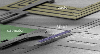
IBM has continued experiments with graphene. The thickness of this material is equal to one atom and has a conductivity of electrons is many times better than silicon. However, many problems remain with the inclusion of graphene in a traditional CMOS process technology. First, it is easy to damage. Secondly, it does not stay on the substrate and on a microscopic level it is not so easy to glue. Recall the summer of 2011, IBM demonstrated a working model of the mixer frequency to a single transistor with graphene channel. The circuit transistor operated at a frequency of 10 GHz. The company noted that the operating parameters of the transistor could be better. Graphene device performance significantly worsened imperfect production technology. To date, the company developed a manufacturing process that does not lead to a deterioration of parameters. This allowed the claim that the new channel transistors from graphene demonstrate the true potential of promising material. They were in a 10 thousand (!) Times more productive than the previous experimental solutions.  As proof of the successful development of new technology, IBM demonstrated a 200-mm plate with RF circuits based on graphene FETs. The circuit comprises three transistors, four coils, two capacitors and two resistors. Each unit occupies a surface area of 0.6 m. mm. Miniature transmitter with radio path of graphene transistors (made of graphene only channel FETs) successfully transmitted over the radio frequency of 4.3 GHz signal text, which was encrypted name of the company: (IBM).
Whether it comes to processors? Obviously, it comes. But it will not be soon. At first channel transistors from graphene is tempting to use a miniature radio frequency circuits. HPC consume significantly less than pure silicon circuits. And, of course, the development of IBM immediately go to the main sponsor of the project - DARPA organization . Related Products : | ||
|
|
||
|
xtreview is your : Video card - cpu - memory - Hard drive - power supply unit source |
|
|
|
|
||
|
Xtreview Support  N-Post:xxxx Xtreview Support        |
IBM DEMONSTRATED GRAPHENE TRANSISTORS TRANSMITTER |
| Please Feel Free to write any Comment; Thanks  |
HTC U 11 on Snapdragon 835 demonstrated a promising result in GeekBench (2017-04-30)
MSI demonstrated automatic overclocking Kaby Lake up to 5.2 GHz (2017-01-18)
AMD demonstrated the possibility Ryzen processor Zen (2016-12-14)
Console Nintendo Switch demonstrated live (2016-12-10)
AMD has already demonstrated new products to a narrow circle of people (2016-12-09)
Intel demonstrated Broadwell-EP processors with built-in dies Altera (2016-11-17)
NVIDIA demonstrated a mobile Quadro on GPU Pascal (2016-07-27)
Boston Dynamics has demonstrated the possibility of domestic four-legged robot (2016-06-24)
At Computex 2016 demonstrated a motherboard with integrated GeForce GTX 1070 (2016-06-05)
At Computex 2016, AMD demonstrated the processor Summit Ridge Zen (2016-06-01)
AMD demonstrated the possibility of Polaris 10 in Doom QuadHD (2016-05-30)
Working NVIDIA Pascal samples can be demonstrated in early April (2016-02-24)
dual Fiji system was demonstrated on Los Angeles (2016-01-25)
Google demonstrated a robot-car sled (2015-12-23)
NEC demonstrated drones detection system (2015-10-09)
Quad GeForce GTX 980 Ti once again demonstrated the power of water cooling in Catzilla (2015-09-15)
At Computex 2015 graphics card AMD Fury demonstrated only partners to the company (2015-06-06)
AMD demonstrated its FreeSync via HDMI (2015-06-06)
Intel demonstrated a sample tablet on Skylake processor (2015-06-03)
OCZ announced new SSD-drives Trion 100 on TLC NAND memory and demonstrated NVMe SSD (2015-06-02)
![]()
To figure out your best laptops .Welcome to XTreview.com. Here u can find a complete computer hardware guide and laptop rating .More than 500 reviews of modern PC to understand the basic architecture


7600gt review
7600gt is the middle card range.
We already benchmarked this video card and found that ...

 geforce 8800gtx and 8800gts
  Xtreview software download Section
  AMD TURION 64 X2 REVIEW
  INTEL PENTIUM D 920 , INTEL PENTIUM D 930
  6800XT REVIEW
  computer hardware REVIEW
  INTEL CONROE CORE DUO 2 REVIEW VS AMD AM2
  INTEL PENTIUM D 805 INTEL D805
  Free desktop wallpaper
  online fighting game
  Xtreview price comparison center
 Lastest 15 Reviews


Rss Feeds
Last News
- The new version of GPU-Z finally kills the belief in the miracle of Vega transformation
- The motherboard manufacturer confirms the characteristics of the processors Coffee Lake
- We are looking for copper coolers on NVIDIA Volta computing accelerators
- Unofficially about Intels plans to release 300-series chipset
- The Japanese representation of AMD offered monetary compensation to the first buyers of Ryzen Threadripper
- This year will not be released more than 45 million motherboards
- TSMC denies the presentation of charges from the antimonopoly authorities
- Radeon RX Vega 64 at frequencies 1802-1000 MHz updated the record GPUPI 1B
- AMD itself would like to believe that mobile processors Ryzen have already been released
- AMD Vega 20 will find application in accelerating computations
- Pre-orders for new iPhone start next week
- Radeon RX Vega 57, 58 and 59: the wonders of transformation
- ASML starts commercial delivery of EUV-scanners
- The older Skylake processors with a free multiplier are removed from production
- Meizu will release Android-smartphone based on Helio P40
- AMD Bristol Ridge processors are also available in American retail
- The fate of Toshiba Memory can be solved to the next environment
- duo GeForce GTX 1080 Ti in GPUPI 1B at frequencies of 2480-10320 MHz
- New Kentsfield overclocking record up to 5204 MHz
- Lenovo released Android-smartphone K8

HALO 3 HALO 3 - Final Fight!

PREY Prey is something you don t often see anymore: a totally unigue shooter experience.

computer news computer parts review Old Forum Downloads New Forum Login Join Articles terms Hardware blog Sitemap Get Freebies


