OOPS! You forgot to upload swfobject.js ! You must upload this file for your form to work.
Cobalt save copper connections of up to 10 nm
![]()
|
xtreview is your : Video card - cpu - memory - Hard drive - power supply unit source |
|
|||
|
|
||||
 Recommended : Free unlimited image hosting with image editor
|
POSTER: computer news || COBALT SAVE COPPER CONNECTIONS OF UP TO 10 NM |
DATE:2014-05-18 |
|
|
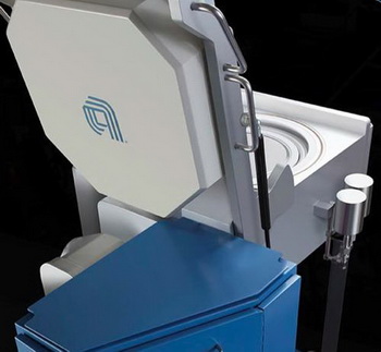
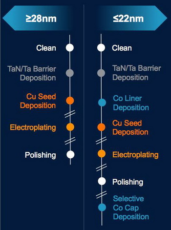
The last ten years, the manufacturers are switching to copper compound semiconductors. Prior to this, for such purposes unused aluminum. But copper is also close to the limit of their capabilities. The finer process technology, the higher the probability of formation of shells and the more intense the process of diffuse infiltration of copper into the dielectric - electromigration. As a result, the defect rate in the production increases, and decreases as the semiconductor lifetime. Recently, copper compounds was used to protect the barrier of tantalum and tantalum nitride (TaN / T). Applied Materials company offered to cover additional layer of cobalt copper connections. According to their estimates, cobalt layer on the order reduces the rate of electromigration of copper atoms in the material boundary. Individual partners note that the rate of electromigration in some cases was reduced by two .  Encapsulation of copper in cobalt company Applied Materials proposes to use its platform Endura Volta. This arrangement is already used for cleaning debris from the wafer after processing. The process of applying cobalt in two stages to increase the technological chain of steps required to process each wafer. However, increase in the reliability of electronic circuits compensate for the increase in cost.  Related Products : | ||
|
|
||
|
xtreview is your : Video card - cpu - memory - Hard drive - power supply unit source |
|
|
|
|
||
|
Xtreview Support  N-Post:xxxx Xtreview Support        |
COBALT SAVE COPPER CONNECTIONS OF UP TO 10 NM |
| Please Feel Free to write any Comment; Thanks  |
Rejecting the idea of releasing ARM server processor , could save AMD about 25 million (2017-05-12)
The Danish data center of Apple will save neighboring farmers from waste (2017-04-21)
Manufacturers of video cards believe that AMD Vega will save the market (2017-04-13)
Intel has shown a willingness to save on paper and cardboard packaging (2017-01-21)
Crytek saved game The Climb from Denuvo protectio (2016-12-12)
Intel admits that will save on development of client products (2016-11-30)
AMD offers to save the world, going to the Radeon RX 480 (2016-08-24)
Intel promises not to save when restructuring (2016-04-20)
Foxconn hopes to save on the purchase of Sharp (2016-03-26)
Google robocar will save on roads, parking lots and public transportation (2016-03-15)
Japanese forces will have to save Sharp (2016-01-28)
Laptops Xiaomi save on components of the latest generation (2015-12-26)
Reinforcing plate Aqua Computer will save up scalped Skylake processors (2015-12-22)
Scythe is ready to save Skylake CPU from killer coolers (2015-11-27)
Tim Cook said that Apple Watch save lives (2015-10-28)
Carbon nanotubes IBM save Moores Law (2015-10-03)
iPhone 5c saved its owner from a gunshot (2015-05-24)
Japanese banks from bankruptcy save Sharp (2015-05-15)
Intel is going to save on paper instructions for boxed processors (2015-03-12)
Smart helmet for cyclists will allow Volvo to save more lives (2014-12-22)
![]()
To figure out your best laptops .Welcome to XTreview.com. Here u can find a complete computer hardware guide and laptop rating .More than 500 reviews of modern PC to understand the basic architecture


7600gt review
7600gt is the middle card range.
We already benchmarked this video card and found that ...

 geforce 8800gtx and 8800gts
  Xtreview software download Section
  AMD TURION 64 X2 REVIEW
  INTEL PENTIUM D 920 , INTEL PENTIUM D 930
  6800XT REVIEW
  computer hardware REVIEW
  INTEL CONROE CORE DUO 2 REVIEW VS AMD AM2
  INTEL PENTIUM D 805 INTEL D805
  Free desktop wallpaper
  online fighting game
  Xtreview price comparison center
 Lastest 15 Reviews


Rss Feeds
Last News
- The new version of GPU-Z finally kills the belief in the miracle of Vega transformation
- The motherboard manufacturer confirms the characteristics of the processors Coffee Lake
- We are looking for copper coolers on NVIDIA Volta computing accelerators
- Unofficially about Intels plans to release 300-series chipset
- The Japanese representation of AMD offered monetary compensation to the first buyers of Ryzen Threadripper
- This year will not be released more than 45 million motherboards
- TSMC denies the presentation of charges from the antimonopoly authorities
- Radeon RX Vega 64 at frequencies 1802-1000 MHz updated the record GPUPI 1B
- AMD itself would like to believe that mobile processors Ryzen have already been released
- AMD Vega 20 will find application in accelerating computations
- Pre-orders for new iPhone start next week
- Radeon RX Vega 57, 58 and 59: the wonders of transformation
- ASML starts commercial delivery of EUV-scanners
- The older Skylake processors with a free multiplier are removed from production
- Meizu will release Android-smartphone based on Helio P40
- AMD Bristol Ridge processors are also available in American retail
- The fate of Toshiba Memory can be solved to the next environment
- duo GeForce GTX 1080 Ti in GPUPI 1B at frequencies of 2480-10320 MHz
- New Kentsfield overclocking record up to 5204 MHz
- Lenovo released Android-smartphone K8

HALO 3 HALO 3 - Final Fight!

PREY Prey is something you don t often see anymore: a totally unigue shooter experience.

computer news computer parts review Old Forum Downloads New Forum Login Join Articles terms Hardware blog Sitemap Get Freebies


