OOPS! You forgot to upload swfobject.js ! You must upload this file for your form to work.
IBM reported a breakthrough in the development of the technical process with a rate of 5 nm
![]()
|
xtreview is your : Video card - cpu - memory - Hard drive - power supply unit source |
|
|||
|
|
||||
 Recommended : Free unlimited image hosting with image editor
|
POSTER: computer news || IBM REPORTED A BREAKTHROUGH IN THE DEVELOPMENT OF THE TECHNICAL PROCESS WITH A RATE OF 5 NM |
DATE:2017-06-06 |
|
|
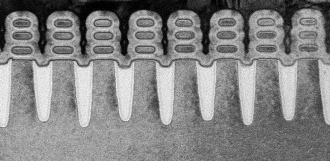
A couple of weeks ago, Samsung admitted that risky production with a 5-nm standard will begin in 2019. True, the emphasis during the report on the development of new technical processes was made on a 4-nm production rate, but this does not change the essence. Transistors with 4 and 5 nm standards will get a new structure. At Samsung, it's called the multi-bridge channel FET or MBCFET. Externally, this is the same silicon fin FinFET, only now it is not integral. The silicon channel
from the monolithic rib turned into several silicon jumpers (they can be seen in the section on the photo below), surrounded on all sides by the shutter material. This significantly increased the gate area and the ability to adjust the currents, and significantly reduced leakage.  "Responsibility" for the development of MBCFET or, in general, GAAFET (gate-all-around FET), was taken over by IBM. The development was told yesterday at the VLSI Technology and Circuits conference in Kyoto, Japan. The development was carried out in cooperation with GlobalFoundries and Samsung, based on the IBM Research Alliance. From this it follows that the transistors MBCFET with the norms of 5 nm will produce both Samsung and GlobalFoundries. IBM is confident that this is a revolutionary invention among the many others that the company has made in its history.  According to the developers, smartphones on the 5-nm element base will be able to work without recharging for 2-3 days. More intelligible formulations explain that, in comparison with the 7-nm FinFET process technology, the performance of a 5-nm process with channels in the form of "nanoprawels" will grow by up to 40%. With the same performance, the power consumption of 5-nm chips will be 75% less than 10-nm chips. The density of transistors placement will also increase. So, using an experienced 7 nm process technology, IBM released a chip with 20 billion transistors two years ago. The process technology of 5 nm will allow to place up to 30 billion transistors on the same area of the crystal. Let's add, for release of 5-nm decisions on the base of transistors from nanostranits and surrounding shutters EUV-lithography will be used. By this time, lithography with a wavelength of 13.5 nm manufacturers run on the technical process with the norms of 7 nm and, apparently, 6 nm. In any case, even today all these partners were able to implement in silicon, although it is hardly a question of working chips. Related Products : | ||
|
|
||
|
xtreview is your : Video card - cpu - memory - Hard drive - power supply unit source |
|
|
|
|
||
|
Xtreview Support  N-Post:xxxx Xtreview Support        |
IBM REPORTED A BREAKTHROUGH IN THE DEVELOPMENT OF THE TECHNICAL PROCESS WITH A RATE OF 5 NM |
| Please Feel Free to write any Comment; Thanks  |
IBM reported a breakthrough in the development of the technical process with a rate of 5 nm (2017-06-06)
Backblaze reported on the failure of hard drives in the third quarter (2016-12-08)
ASML reported the timing of EUV-lithography introduction in the manufacture of memory (2016-10-20)
IBM and Samsung have reported the development of 11-nm memory STT MRAM (2016-07-08)
EVGA reported the price of GeForce GTX 1080 Founders Edition (2016-05-11)
A9 processors Manufacturer for the iPhone 6s reported record earnings (2016-01-15)
Intel reported a record revenue (2015-01-16)
Samsung reported about the latest NFC-chip (2014-12-01)
NVIDIA reported about the Android-tablet Nexus 9 (2014-09-11)
MSI reported new extreme overclocking records (2014-09-02)
LG reported about second quarter results (2014-07-24)
G.Skill reported about six records of extreme overclocking (2014-06-17)
Western Digital has reported the results of the quarter (2014-05-02)
TSMC reported first quarter results (2014-04-18)
Apple reported a record quarter, the stock fell 8 percents (2014-01-28)
Western Digital has reported on the results of the quarter (2014-01-23)
Amazon reported record sales of Kindle devices (2013-12-05)
MediaTek has reported on progress in the second quarter of 2013 (2013-08-04)
Intel reported the name of another client to the contract semiconductors (2013-05-03)
Barnes and Noble reported about the decline in sales of devices for reading (2013-03-01)
![]()
To figure out your best laptops .Welcome to XTreview.com. Here u can find a complete computer hardware guide and laptop rating .More than 500 reviews of modern PC to understand the basic architecture


7600gt review
7600gt is the middle card range.
We already benchmarked this video card and found that ...

 geforce 8800gtx and 8800gts
  Xtreview software download Section
  AMD TURION 64 X2 REVIEW
  INTEL PENTIUM D 920 , INTEL PENTIUM D 930
  6800XT REVIEW
  computer hardware REVIEW
  INTEL CONROE CORE DUO 2 REVIEW VS AMD AM2
  INTEL PENTIUM D 805 INTEL D805
  Free desktop wallpaper
  online fighting game
  Xtreview price comparison center
 Lastest 15 Reviews


Rss Feeds
Last News
- The new version of GPU-Z finally kills the belief in the miracle of Vega transformation
- The motherboard manufacturer confirms the characteristics of the processors Coffee Lake
- We are looking for copper coolers on NVIDIA Volta computing accelerators
- Unofficially about Intels plans to release 300-series chipset
- The Japanese representation of AMD offered monetary compensation to the first buyers of Ryzen Threadripper
- This year will not be released more than 45 million motherboards
- TSMC denies the presentation of charges from the antimonopoly authorities
- Radeon RX Vega 64 at frequencies 1802-1000 MHz updated the record GPUPI 1B
- AMD itself would like to believe that mobile processors Ryzen have already been released
- AMD Vega 20 will find application in accelerating computations
- Pre-orders for new iPhone start next week
- Radeon RX Vega 57, 58 and 59: the wonders of transformation
- ASML starts commercial delivery of EUV-scanners
- The older Skylake processors with a free multiplier are removed from production
- Meizu will release Android-smartphone based on Helio P40
- AMD Bristol Ridge processors are also available in American retail
- The fate of Toshiba Memory can be solved to the next environment
- duo GeForce GTX 1080 Ti in GPUPI 1B at frequencies of 2480-10320 MHz
- New Kentsfield overclocking record up to 5204 MHz
- Lenovo released Android-smartphone K8

HALO 3 HALO 3 - Final Fight!

PREY Prey is something you don t often see anymore: a totally unigue shooter experience.

computer news computer parts review Old Forum Downloads New Forum Login Join Articles terms Hardware blog Sitemap Get Freebies


