OOPS! You forgot to upload swfobject.js ! You must upload this file for your form to work.
Russian scientists presented ferroelectric MELRAM
![]()
|
xtreview is your : Video card - cpu - memory - Hard drive - power supply unit source |
|
|||
|
|
||||
 Recommended : Free unlimited image hosting with image editor
|
POSTER: computer news || RUSSIAN SCIENTISTS PRESENTED FERROELECTRIC MELRAM |
DATE:2017-08-27 |
|
|
Recently in the journal Applied Physics Letters was published an article devoted to the development of the structure of ferroelectric nonvolatile memory or MELRAM (magnetoelectric RAM). The development, was created by Russian scientists in collaboration with French scientists. In the design and prototype development , specialists from the Moscow Physicotechnical Institute (MFTI), VA Kotelnikov Institute of Radio Engineering and Electronics of the Russian Academy of Sciences and the
International Associate Laboratory LIA LICS were engaged. In the future, it turns out to create a cell on a nanometer scale, and the prototype measures about one millimeter, there is hope to see a magnetoresistive memory much simpler in structure than the modern ReRAM with complex magnetoresistive tunnel junctions. But the main goal is the dream that MELRAM will be able to replace the DRAM in the future. The latter, as is known, requires a constant procedure for data regeneration, since the unit cell DRAM is a banal capacitor with control from a
transistor. Memory MELRAM, on the contrary, will be non-volatile and consumes little. Researchers talk about a potential of 10,000 times and even more reduce the consumption of the memory cell in case of switching to MELRAM. However, while there are problems with energy independence. For the early prototypes, large magnetic field sensors were used to read the data, which is simply impossible to scale. Data from the cell of the new prototype is read using short pulses, as is customary for ReRAM.
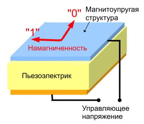
However, during the reading process, the data in the cells are destroyed (this is the nature of the cell) and a data regeneration operation is required. This will reduce the energy efficiency limits of the MELRAM cell, but among the 10,000-fold prize this will be invisible.  As for the structure of MELRAM, it is the following. The basic element of the cell is a piezoelectric material. The piezoelectric is different in that it can produce stress in the event of physical deformation and deform in the event of a voltage supply. This is the MELRAM control. A memory element of MELRAM was a multi-layered construction on the surface of a piezoelectric - several layers of terbium and cobalt (TbCo2) and a layer of iron and cobalt (FeCo). Under the action of a deforming piezoelectric, the multilayer magnetoelastic design changes the direction of magnetization. Depending on the magnetic field vector, this can be interpreted as "0" or as "1", which is equivalent to writing to a cell in the data bit. Development is in the early stages of research. The current dimensions of the prototype do not allow to hope for the rapid appearance of significantly improved elements of MELRAM. Related Products : | ||
|
|
||
|
xtreview is your : Video card - cpu - memory - Hard drive - power supply unit source |
|
|
|
|
||
|
Xtreview Support  N-Post:xxxx Xtreview Support        |
RUSSIAN SCIENTISTS PRESENTED FERROELECTRIC MELRAM |
| Please Feel Free to write any Comment; Thanks  |
Russian scientists presented ferroelectric MELRAM (2017-08-27)
Another Russian overclocker successfully debuted in the overclocking of Intel X299 platform (2017-08-07)
Gartner saw signs of improvement in the Russian PC market (2017-07-13)
The new video on Quake Champions was dedicated to the victim of Russian special services Visor (2017-05-11)
Russians have already started overclocking Radeon RX 580 (2017-04-21)
Russian showed 15 best results of overclocking Radeon RX 460 (2017-04-09)
The pair Radeon R9 290 allowed the Russian to set 9 records in the model standings (2017-03-26)
In the last half of the years Russians are willing to buy laptops (2017-01-19)
The Russian showed the best for the GeForce GTX 1080 results in 3DMark11 Performance (2016-09-10)
Acer introduced in the Russian market notebooks Aspire S 13 and Aspire Switch 12 Alpha (2016-05-30)
Russian companies continue to develop the core architecture and Imagination (2016-05-25)
New Russian thermal grease (2016-05-08)
Russian scientists a hundred times speeded superconducting memory (2016-03-24)
Meadowsweet Terminal - the first mass Russian system processors Baikal-T1 (2016-02-25)
Baikal Electronics and Basalt ACT was prepared according to Russian processors (2016-01-27)
Samsung - the most favorite brand of Russians (2015-12-08)
Lenovo is interested in using Russian processors Baikal (2015-09-20)
This year, the Russian market of smartphones will not grow (2015-02-17)
Xiaomi will enter the Russian market in next year (2014-11-25)
Motorola will get sale items on the Russian market in the next year (2014-11-24)
![]()
To figure out your best laptops .Welcome to XTreview.com. Here u can find a complete computer hardware guide and laptop rating .More than 500 reviews of modern PC to understand the basic architecture


7600gt review
7600gt is the middle card range.
We already benchmarked this video card and found that ...

 geforce 8800gtx and 8800gts
  Xtreview software download Section
  AMD TURION 64 X2 REVIEW
  INTEL PENTIUM D 920 , INTEL PENTIUM D 930
  6800XT REVIEW
  computer hardware REVIEW
  INTEL CONROE CORE DUO 2 REVIEW VS AMD AM2
  INTEL PENTIUM D 805 INTEL D805
  Free desktop wallpaper
  online fighting game
  Xtreview price comparison center
 Lastest 15 Reviews


Rss Feeds
Last News
- The new version of GPU-Z finally kills the belief in the miracle of Vega transformation
- The motherboard manufacturer confirms the characteristics of the processors Coffee Lake
- We are looking for copper coolers on NVIDIA Volta computing accelerators
- Unofficially about Intels plans to release 300-series chipset
- The Japanese representation of AMD offered monetary compensation to the first buyers of Ryzen Threadripper
- This year will not be released more than 45 million motherboards
- TSMC denies the presentation of charges from the antimonopoly authorities
- Radeon RX Vega 64 at frequencies 1802-1000 MHz updated the record GPUPI 1B
- AMD itself would like to believe that mobile processors Ryzen have already been released
- AMD Vega 20 will find application in accelerating computations
- Pre-orders for new iPhone start next week
- Radeon RX Vega 57, 58 and 59: the wonders of transformation
- ASML starts commercial delivery of EUV-scanners
- The older Skylake processors with a free multiplier are removed from production
- Meizu will release Android-smartphone based on Helio P40
- AMD Bristol Ridge processors are also available in American retail
- The fate of Toshiba Memory can be solved to the next environment
- duo GeForce GTX 1080 Ti in GPUPI 1B at frequencies of 2480-10320 MHz
- New Kentsfield overclocking record up to 5204 MHz
- Lenovo released Android-smartphone K8

HALO 3 HALO 3 - Final Fight!

PREY Prey is something you don t often see anymore: a totally unigue shooter experience.

computer news computer parts review Old Forum Downloads New Forum Login Join Articles terms Hardware blog Sitemap Get Freebies


