OOPS! You forgot to upload swfobject.js ! You must upload this file for your form to work.
Texas Instrument could not change the order of new production methods introduction
![]()
|
xtreview is your : Video card - cpu - memory - Hard drive - power supply unit source |
|
|||
|
|
||||
 Recommended : Free unlimited image hosting with image editor
|
POSTER: computer news || TEXAS INSTRUMENT COULD NOT CHANGE THE ORDER OF NEW PRODUCTION METHODS INTRODUCTION |
DATE:2012-12-19 |
|
|
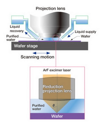
Replaced by modern manufacturing projection equipment based on 193-nm laser could reach 157-nm projection as recognized technologist Texas Instrument, Jim Blatchford . At the time, the company has negotiated with manufacturers of tools, during which there has been some consensus. When it came time to discuss the standards, an industry group of developers - SPIE, Society of Photo-Optical Instrumentation Engineers - opted for immersion (immersion) lithography. The possibility to increase the resolution of microscope by placing the fluid between the lens and the subject was proved in the seventeenth century by English naturalist Robert Hooke . Three hundred years later, these microscopes have emerged as a daily working tool in all scientific laboratories. Thus, the resolution of the projection is increased by a significant amount without reducing the wavelength of the laser projection.  First immersion lithography in 2005, is widely used by TSMC company , applying it to the production of 65-nm semiconductor. AMD has moved to immersion projection method applied to 45-nm solutions, and Intel company - the implementation phase of 32-nm semiconductor. At the same time to reduce the size of an element on the chip was used as a turn-based projection with two and even three photomasks. To date, TI plans to move to less risky 157-nm projection , and in fact it could have been different ... Limit of 193-nm immersion lithography some call 8-nm process technology, others - 5-nm and even 3 nm. But its ability to take out, as they say, to the bottom - it can cost a pretty serious money. This year well invested Intel, Samsung and TSMC company. This gives a certain chance that in two or three years of commercial EUV-projection can speak more confidently. While skeptics have criticized both the expected life time of the 193 nm immersion lithography, and the earliest possible commissioning of EUV-lithography. Related Products : | ||
|
|
||
|
xtreview is your : Video card - cpu - memory - Hard drive - power supply unit source |
|
|
|
|
||
|
Xtreview Support  N-Post:xxxx Xtreview Support        |
TEXAS INSTRUMENT COULD NOT CHANGE THE ORDER OF NEW PRODUCTION METHODS INTRODUCTION |
| Please Feel Free to write any Comment; Thanks  |
Refusal of the instrument panel facilitated night driving in the Tesla Model 3 (2017-07-24)
Texas Instruments can acquire AMD (2017-04-06)
Texas Instruments can absorb Maxim Integrated Products (2015-11-02)
Texas Instruments sees no need for acquisitions and mergers (2015-10-25)
Texas Instruments can absorb some competitors (2015-06-21)
Texas Instruments helps wearable devices to receive additional energy (2014-12-23)
Texas Instrument could not change the order of new production methods introduction (2012-12-19)
Audi will use Texas Instruments processors in the information systems of its vehicles (2012-12-14)
Texas Instruments will pay more attention to the technology of wireless charging (2012-12-10)
Intel competes with Apple for retired professionals from Texas Instruments (2012-12-07)
Apple will employ laid-off engineers from Texas Instruments (2012-12-05)
Logic Instrument Fieldbook A2 (2012-12-03)
Texas Instruments ceased developing platforms for smartphones and tablets (2012-11-15)
Texas Instruments will release special server on ARM SoC (2012-11-14)
Texas Instruments makes wireless charging easier (2012-11-07)
Texas Instruments demonstrates tablet costing no more than 70 dollars (2012-11-01)
Amazon may buy Texas Instruments processor business (2012-10-15)
Texas Instruments no longer invest in the development of smartphones processors (2012-09-27)
Texas Instruments lowers interest in smartphones and tablets (2012-09-14)
Texas Instruments was faced with a reduction of orders for its products (2012-07-24)
![]()
To figure out your best laptops .Welcome to XTreview.com. Here u can find a complete computer hardware guide and laptop rating .More than 500 reviews of modern PC to understand the basic architecture


7600gt review
7600gt is the middle card range.
We already benchmarked this video card and found that ...

 geforce 8800gtx and 8800gts
  Xtreview software download Section
  AMD TURION 64 X2 REVIEW
  INTEL PENTIUM D 920 , INTEL PENTIUM D 930
  6800XT REVIEW
  computer hardware REVIEW
  INTEL CONROE CORE DUO 2 REVIEW VS AMD AM2
  INTEL PENTIUM D 805 INTEL D805
  Free desktop wallpaper
  online fighting game
  Xtreview price comparison center
 Lastest 15 Reviews


Rss Feeds
Last News
- The new version of GPU-Z finally kills the belief in the miracle of Vega transformation
- The motherboard manufacturer confirms the characteristics of the processors Coffee Lake
- We are looking for copper coolers on NVIDIA Volta computing accelerators
- Unofficially about Intels plans to release 300-series chipset
- The Japanese representation of AMD offered monetary compensation to the first buyers of Ryzen Threadripper
- This year will not be released more than 45 million motherboards
- TSMC denies the presentation of charges from the antimonopoly authorities
- Radeon RX Vega 64 at frequencies 1802-1000 MHz updated the record GPUPI 1B
- AMD itself would like to believe that mobile processors Ryzen have already been released
- AMD Vega 20 will find application in accelerating computations
- Pre-orders for new iPhone start next week
- Radeon RX Vega 57, 58 and 59: the wonders of transformation
- ASML starts commercial delivery of EUV-scanners
- The older Skylake processors with a free multiplier are removed from production
- Meizu will release Android-smartphone based on Helio P40
- AMD Bristol Ridge processors are also available in American retail
- The fate of Toshiba Memory can be solved to the next environment
- duo GeForce GTX 1080 Ti in GPUPI 1B at frequencies of 2480-10320 MHz
- New Kentsfield overclocking record up to 5204 MHz
- Lenovo released Android-smartphone K8

HALO 3 HALO 3 - Final Fight!

PREY Prey is something you don t often see anymore: a totally unigue shooter experience.

computer news computer parts review Old Forum Downloads New Forum Login Join Articles terms Hardware blog Sitemap Get Freebies


