ASML is confident in the superiority of EUV-lithography, but fears for the fate of the 450-mm production

|
xtreview is your : Video card - cpu - memory - Hard drive - power supply unit source |
|
|||
|
|
||||


 Recommended : Free unlimited image hosting with image editor
|
POSTER: computer news || ASML IS CONFIDENT IN THE SUPERIORITY OF EUV-LITHOGRAPHY, BUT FEARS FOR THE FATE OF THE 450-MM PRODUCTION |
DATE:2013-02-20 |
|
|
Yesterday began the Annual Conference of International Solid-State Circuits Conference (ISSCC 2013). In their experiments, ASML failed to prove in practice that the radiation in the ultraviolet range of ultra-rigid to control and further optimization. Emulation of a continuous cycle with 40-watt light source allowed to enter the theoretical performance figures of 165 wafers per hour with a level of 0.01% . The company also conducted an experiment which could control 60-watt light source for 40 hours, and it gave a stable result. 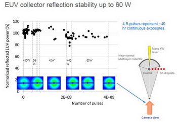 Today, the theoretical limit of performance for the production of wafers up to 250 plates per hour. Transition to EUV-projection, so will be accompanied by a decrease in production and an increase in production costs. Since the beginning of EUV-production in 2014, promises to achieve the performance of scanners 70 plates per hour. Radiation power at the same is unlikely to exceed 60 watts. Ideally, the developer should bring output power up to 250 W, but even with such power the working performance of EUV-scanners will remain at a level of 100 wafers per hour. According to ASML, the most appropriate to deploy EUV-scanner will move to 10-nm process. Such production would require only one photomask for projection. Intel company , for example, believe that the 10-nm semiconductor can produce with the old equipment and four-five photomasks. However, Intel has invested enormous resources in developing EUV-equipment and bought a stake in ASM. As calculated ASML, even triple projection ceases to be profitable and easy to use. 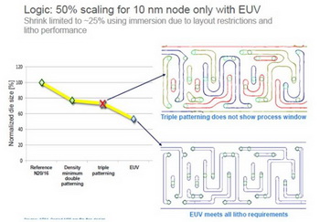 To further reduce the scale of production methods, however, in considering options for ASML double and triple exposure for 7-nm level and 3 nm. In addition, the variants on the serial reduction wavelength optics and improve the transition to self-organizing structures. It is assumed that the first 450-mm equipment will work in 2018 on the second generation EUV-scanners.
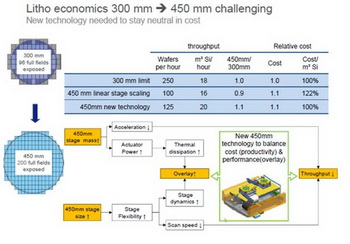 In the calculations presented by the relative price of a square meter on 450-mm wafers can be 22% higher than in the case of 300-mm wafers. Situation promises equalized with the transition to a brand new 450-mm equipment that will be installed on new production, originally targeted for processing 450-mm wafers. In other words, the greatest effect will be on those factories to be built from scratch and without the use of, let's say, a 300-mm infrastructure. This is not just lithography equipment, but also the entire organization of production, from bringing up, storage and supply of plates and finishing systems and other water treatment . Related Products : | ||
|
|
||
|
xtreview is your : Video card - cpu - memory - Hard drive - power supply unit source |
|
|
|
|
||
|
Xtreview Support  N-Post:xxxx Xtreview Support  |
ASML IS CONFIDENT IN THE SUPERIORITY OF EUV-LITHOGRAPHY, BUT FEARS FOR THE FATE OF THE 450-MM PRODUCTION |
| Please Feel Free to write any Comment; Thanks  |
The motherboard manufacturer confirms the characteristics of the processors Coffee Lake (2017-09-08)
This year will not be released more than 45 million motherboards (2017-09-08)
AMD Bristol Ridge processors are also available in American retail (2017-09-07)
Advertising Radeon RX 570 for 279 dollars AMD caused a storm of emotions (2017-09-07)
In exchange for increasing the stake in the joint venture with Toshiba, Western Digital Corporation is ready to refuse to participate in the auction (2017-09-06)
AMD gave details about the history of the Ryzen Threadripper (2017-09-06)
The characteristics of the mobile chip MediaTek Helio P40 are known (2017-09-06)
AMD processors with Zen architecture of the second generation will raise frequencies and specific performance (2017-09-05)
Memory manufacturers increased capital costs this year (2017-09-04)
Retail boxed versions of economical processors Bristol Ridge (2017-09-03)
Specifications PCIe 4.0 will see the light this year, and PCIe 5.0 in 2019 (2017-08-30)
Intel introduced Movidius Myriad X the visual center for robots became smarter (2017-08-29)
A new round of video card price hike is triggered by a rise in prices for memory chips (2017-08-28)
The decision on the transaction between WDC and Toshiba can be made on August 31 (2017-08-27)
Russian scientists presented ferroelectric MELRAM (2017-08-27)
In pursuit of Toshiba Memory assets, Western Digital Corporation is ready to give up voting rights (2017-08-25)
In the second quarter, miners broke the sales statistics of video cards (2017-08-25)
Former CFO Intel is preparing to leave the company (2017-08-25)
Quake Champions is now available to all comers in the early access of Steam (2017-08-23)
AMD promises to do everything possible to return prices for Radeon RX Vega to the recommended level (2017-08-23)

To figure out your best laptops .Welcome to XTreview.com. Here u can find a complete computer hardware guide and laptop rating .More than 500 reviews of modern PC to understand the basic architecture


7600gt review
7600gt is the middle card range.
We already benchmarked this video card and found that ...
 geforce 8800gtx and 8800gts Xtreview software download Section AMD TURION 64 X2 REVIEW INTEL PENTIUM D 920 , INTEL PENTIUM D 930 6800XT REVIEW computer hardware REVIEW INTEL CONROE CORE DUO 2 REVIEW VS AMD AM2 INTEL PENTIUM D 805 INTEL D805 Free desktop wallpaper online fighting game Xtreview price comparison center
Rss Feeds


- The new version of GPU-Z finally kills the belief in the miracle of Vega transformation
- The motherboard manufacturer confirms the characteristics of the processors Coffee Lake
- We are looking for copper coolers on NVIDIA Volta computing accelerators
- Unofficially about Intels plans to release 300-series chipset
- The Japanese representation of AMD offered monetary compensation to the first buyers of Ryzen Threadripper
- This year will not be released more than 45 million motherboards
- TSMC denies the presentation of charges from the antimonopoly authorities
- Radeon RX Vega 64 at frequencies 1802-1000 MHz updated the record GPUPI 1B
- AMD itself would like to believe that mobile processors Ryzen have already been released
- AMD Vega 20 will find application in accelerating computations
- Pre-orders for new iPhone start next week
- Radeon RX Vega 57, 58 and 59: the wonders of transformation
- ASML starts commercial delivery of EUV-scanners
- The older Skylake processors with a free multiplier are removed from production
- Meizu will release Android-smartphone based on Helio P40
- AMD Bristol Ridge processors are also available in American retail
- The fate of Toshiba Memory can be solved to the next environment
- duo GeForce GTX 1080 Ti in GPUPI 1B at frequencies of 2480-10320 MHz
- New Kentsfield overclocking record up to 5204 MHz
- Lenovo released Android-smartphone K8












computer news computer parts review Old Forum Downloads New Forum Login Join Articles terms Hardware blog Sitemap Get Freebies


