OOPS! You forgot to upload swfobject.js ! You must upload this file for your form to work.
Belgian scientists will help to reduce the scale of NAND-flash below 20 nm
![]()
|
xtreview is your : Video card - cpu - memory - Hard drive - power supply unit source |
|
|||
|
|
||||
 Recommended : Free unlimited image hosting with image editor
|
POSTER: computer news || BELGIAN SCIENTISTS WILL HELP TO REDUCE THE SCALE OF NAND-FLASH BELOW 20 NM |
DATE:2013-06-23 |
|
|
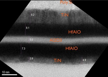
The Belgian research center IMEC at the May conference International Memory Workshop in 2013 proved that Europe still understood something in semiconductors. Scientists from the Old World have made a report in which talked about the possibility of producing a reliable flash memory with less than 20 nm. The main problem with flash chips that cell to maintain charge becomes so small, and the insulating layer is so thin and small in size, that the performance of the flash memory start to deteriorate. This leads to a reduction of rewrites, and the loss of data. Scientists proposed to create a three-layer dielectric between the floating gate and the control transistor cell.  As the interlayer insulating layer, a combination of aluminum oxide (Al2O3) with low dielectric constant (low-k) and two "wrappers" combination of layers of aluminum and hafnium oxide (HfAlO), which are characterized by high dielectric constant (high-k ). High-k/low-k/high-k-izolyatora layer, according to IMEC representatives , "shows excellent results in terms of reliability and retention of the charge." Scientists believe that the three-layer dielectric process technology will reduce the production of NAND-flash chips based on planar transistors below 20 nm without affecting their performance. However, we have some doubts about the compatibility of a 25-nm insulating layer (10/05/10 nm) with a 14-nm and 10-nm transistor gates. Related Products : | ||
|
|
||
|
xtreview is your : Video card - cpu - memory - Hard drive - power supply unit source |
|
|
|
|
||
|
Xtreview Support  N-Post:xxxx Xtreview Support        |
BELGIAN SCIENTISTS WILL HELP TO REDUCE THE SCALE OF NAND-FLASH BELOW 20 NM |
| Please Feel Free to write any Comment; Thanks  |
Russian scientists presented ferroelectric MELRAM (2017-08-27)
Car autopilot inspired scientists to create a navigation system for blind pedestrians (2017-02-07)
Scientists from Berkeley offer cheaper transition to a process technologies with lower standards (2017-01-07)
Scientists have created a copper wire with a diameter of three atoms (2016-12-27)
Scientists have proposed to reduce transistor gate to 1 nm (2016-10-16)
Scientists have made graphene in a light bulb (2016-06-19)
Japanese scientists have created a wearable ultra-thin LED (2016-04-18)
Russian scientists a hundred times speeded superconducting memory (2016-03-24)
Automakers are willing to pay for the development of scientists autopilot (2016-03-17)
Volvo has helped scientists create robot-dustman (2016-02-29)
Australian scientists have developed a bionic spinal cord (2016-02-09)
Scientists have developed a safer lithium-ion batteries (2016-01-12)
Scientists have developed a microprocessor that uses light to transmit data (2015-12-24)
Scientists from Stanford offer to produce multilayer chip (2015-12-19)
Scientists have found a way to split water using solar energy (2015-12-01)
An electronic notebook for scientists (2015-11-25)
Peruvian scientists made a pot plant as power source for lamp (2015-11-24)
Scientists have found yet another way to make lithium-ion batteries better (2015-11-09)
Scientists have found that reading text from the display before bedtime is harmful (2014-12-25)
Scientists say fast charge does not harm the battery (2014-09-16)
![]()
To figure out your best laptops .Welcome to XTreview.com. Here u can find a complete computer hardware guide and laptop rating .More than 500 reviews of modern PC to understand the basic architecture


7600gt review
7600gt is the middle card range.
We already benchmarked this video card and found that ...

 geforce 8800gtx and 8800gts
  Xtreview software download Section
  AMD TURION 64 X2 REVIEW
  INTEL PENTIUM D 920 , INTEL PENTIUM D 930
  6800XT REVIEW
  computer hardware REVIEW
  INTEL CONROE CORE DUO 2 REVIEW VS AMD AM2
  INTEL PENTIUM D 805 INTEL D805
  Free desktop wallpaper
  online fighting game
  Xtreview price comparison center
 Lastest 15 Reviews


Rss Feeds
Last News
- The new version of GPU-Z finally kills the belief in the miracle of Vega transformation
- The motherboard manufacturer confirms the characteristics of the processors Coffee Lake
- We are looking for copper coolers on NVIDIA Volta computing accelerators
- Unofficially about Intels plans to release 300-series chipset
- The Japanese representation of AMD offered monetary compensation to the first buyers of Ryzen Threadripper
- This year will not be released more than 45 million motherboards
- TSMC denies the presentation of charges from the antimonopoly authorities
- Radeon RX Vega 64 at frequencies 1802-1000 MHz updated the record GPUPI 1B
- AMD itself would like to believe that mobile processors Ryzen have already been released
- AMD Vega 20 will find application in accelerating computations
- Pre-orders for new iPhone start next week
- Radeon RX Vega 57, 58 and 59: the wonders of transformation
- ASML starts commercial delivery of EUV-scanners
- The older Skylake processors with a free multiplier are removed from production
- Meizu will release Android-smartphone based on Helio P40
- AMD Bristol Ridge processors are also available in American retail
- The fate of Toshiba Memory can be solved to the next environment
- duo GeForce GTX 1080 Ti in GPUPI 1B at frequencies of 2480-10320 MHz
- New Kentsfield overclocking record up to 5204 MHz
- Lenovo released Android-smartphone K8

HALO 3 HALO 3 - Final Fight!

PREY Prey is something you don t often see anymore: a totally unigue shooter experience.

computer news computer parts review Old Forum Downloads New Forum Login Join Articles terms Hardware blog Sitemap Get Freebies


