OOPS! You forgot to upload swfobject.js ! You must upload this file for your form to work.
Scientists from Berkeley offer cheaper transition to a process technologies with lower standards
![]()
|
xtreview is your : Video card - cpu - memory - Hard drive - power supply unit source |
|
|||
|
|
||||
 Recommended : Free unlimited image hosting with image editor
|
POSTER: computer news || SCIENTISTS FROM BERKELEY OFFER CHEAPER TRANSITION TO A PROCESS TECHNOLOGIES WITH LOWER STANDARDS |
DATE:2017-01-07 |
|
|
Since the beginning of technological processes development with the standards of less than 30 nm began serious difficulties. Costs for the development and implementation began to grow stronger, and the transition process has slowed down and is now available to a limited number of semiconductor manufacturers. For example, each layer for the production of the chip requires two or more photomasks, which in itself is a costly exercise a. Each photomask, must be up to 50 pieces
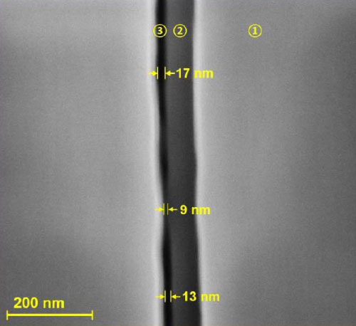
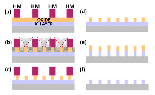
on the SoC and processor today costs about $ 1 million.  Cheaper transition to technical processes with lower standards and return the law of Moore's offer scientists from Berkeley. They have developed so-called process of oblique ion bombardment or TII (tilted ion implantation). The essence of the proposal is clear on the picture. A beam of ions (in particular development - it is a beam of argon ions) aimed at ordinary photomask first from one angle, then from another. The ion beam partially destroys the silicon substrate under the mask and leaves untouched area out of focus. After the usual etching pattern is much less than on the chip than on the photomask. Note, all this takes place in a traditional CMOS process technology that promises affordable transition from the traditional "vertical" projection on the corner. However, manufacturers have not yet lined up for a license to TII.  The presented technology is tested for the production of prototype 9-nm silicon. The resulting projection step is 18-20 nm. For comparison, 7-nm process technology TSMC gives minimum metallization step for the "zero layer" the M0 - the place of first contact with the crystal - as many as 40 nm. In addition, as already mentioned above, TII technology can be up to 50% to reduce the cost of expenses for the development of process technology from 16 nm technological standards, and a 35% increase in chip release performance in a given process technology, which is based on a double projection in normal conditions (uses two mask per layer). Related Products : | ||
|
|
||
|
xtreview is your : Video card - cpu - memory - Hard drive - power supply unit source |
|
|
|
|
||
|
Xtreview Support  N-Post:xxxx Xtreview Support        |
SCIENTISTS FROM BERKELEY OFFER CHEAPER TRANSITION TO A PROCESS TECHNOLOGIES WITH LOWER STANDARDS |
| Please Feel Free to write any Comment; Thanks  |
TSMC denies the presentation of charges from the antimonopoly authorities (2017-09-08)
The older Skylake processors with a free multiplier are removed from production (2017-09-07)
Analysts believe that the new processors from Intel and AMD will revive the PC market in the second half of the year (2017-08-22)
Volkswagen is ready to take the example from Tesla (2017-08-07)
Multiplayer shooter Escape from Tarkov switched to closed beta testing (2017-08-01)
Players will be able to transfer the progress from Wolfenstein The New Order to Wolfenstein II The New Colossus (2017-07-28)
Release Trailer of the role-playing game Pyre from the creators of Bastion and Transistor (2017-07-24)
The Tesla Model 3 killer from Volkswagen will be 7000 dollars cheaper (2017-07-16)
In this quarter, the share of TSMC revenue from 10-nm products will increase dramatically (2017-07-15)
Mass Effect Andromeda is spared from Denuvo (2017-07-10)
Funny video of the building action from Fortune Epic Games (2017-07-10)
Total War Saga - a new line of strategies from the Creative Assembly (2017-07-06)
Micron managed to significantly increase revenue from the implementation of memory for graphics solutions (2017-06-30)
Do you think that society will becaome better or wrose from increased automation and AI (2017-06-29)
NVIDIA believes less in the power of demand for video cards from the miners (2017-06-26)
Ford will teach cars to understand which side the car with flashing lights is coming from (2017-06-25)
Warhammer II dedicated to the map from the story campaign (2017-06-22)
5 minutes of fierce sea battle Skull and Bones from Ubisoft (2017-06-14)
Skull and Bones - promising project for sea battles from Ubisoft (2017-06-13)
In late June, a tool will appear to remove the covers from Skylake-X and Kaby Lake-X (2017-06-13)
![]()
To figure out your best laptops .Welcome to XTreview.com. Here u can find a complete computer hardware guide and laptop rating .More than 500 reviews of modern PC to understand the basic architecture


7600gt review
7600gt is the middle card range.
We already benchmarked this video card and found that ...

 geforce 8800gtx and 8800gts
  Xtreview software download Section
  AMD TURION 64 X2 REVIEW
  INTEL PENTIUM D 920 , INTEL PENTIUM D 930
  6800XT REVIEW
  computer hardware REVIEW
  INTEL CONROE CORE DUO 2 REVIEW VS AMD AM2
  INTEL PENTIUM D 805 INTEL D805
  Free desktop wallpaper
  online fighting game
  Xtreview price comparison center
 Lastest 15 Reviews


Rss Feeds
Last News
- The new version of GPU-Z finally kills the belief in the miracle of Vega transformation
- The motherboard manufacturer confirms the characteristics of the processors Coffee Lake
- We are looking for copper coolers on NVIDIA Volta computing accelerators
- Unofficially about Intels plans to release 300-series chipset
- The Japanese representation of AMD offered monetary compensation to the first buyers of Ryzen Threadripper
- This year will not be released more than 45 million motherboards
- TSMC denies the presentation of charges from the antimonopoly authorities
- Radeon RX Vega 64 at frequencies 1802-1000 MHz updated the record GPUPI 1B
- AMD itself would like to believe that mobile processors Ryzen have already been released
- AMD Vega 20 will find application in accelerating computations
- Pre-orders for new iPhone start next week
- Radeon RX Vega 57, 58 and 59: the wonders of transformation
- ASML starts commercial delivery of EUV-scanners
- The older Skylake processors with a free multiplier are removed from production
- Meizu will release Android-smartphone based on Helio P40
- AMD Bristol Ridge processors are also available in American retail
- The fate of Toshiba Memory can be solved to the next environment
- duo GeForce GTX 1080 Ti in GPUPI 1B at frequencies of 2480-10320 MHz
- New Kentsfield overclocking record up to 5204 MHz
- Lenovo released Android-smartphone K8

HALO 3 HALO 3 - Final Fight!

PREY Prey is something you don t often see anymore: a totally unigue shooter experience.

computer news computer parts review Old Forum Downloads New Forum Login Join Articles terms Hardware blog Sitemap Get Freebies


