Sandy bridge cache system
![]()
|
xtreview is your : Video card - cpu - memory - Hard drive - power supply unit source |
|
|||
|
|
||||

 Recommended : Free unlimited image hosting with image editor
|
POSTER: computer news || SANDY BRIDGE CACHE SYSTEM |
DATE:2010-09-19 |
|
|
One of the primary tasks, which stood before Intel engineers with the development of sandy bridge design, there was to integrate graphic core in one crystal with the processor. For this reason graphic core was completely rebuild-ed and from the processor design side it is simply some more processor core. For connection and interaction of processor core, graphic core and caches is created the new internal bus ring, which works at the fixed frequency : 3 GHz. 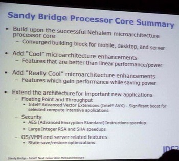 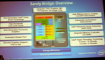 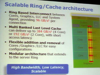 Caches for each processor core now are called Last level cache (LLC). In Sandy bridge the cache of last level (LLC) works at a constant fixed frequency. In this case the latency with the work of cache are reduced and the second port for the data load is introduced. 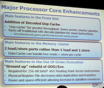 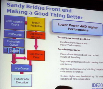 Separately instructions and addresses go from data. 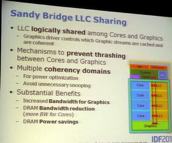 In Sandy bridge was realized a new generation of turbo boost technology, which ensures the acceleration of processor core or graphic core depending on the needs of usable applications. In this case it can overclock to the maximum immediately all processor core, including graphic, but not like the previous generation: 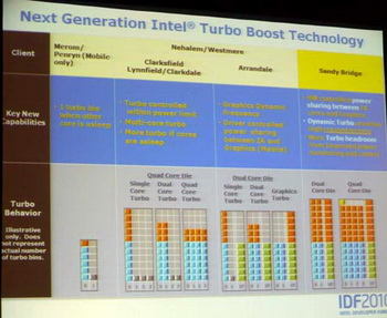 At peak load exceeding max TDP is allowed. 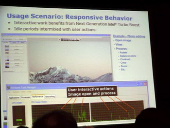 Approximately for 20-25 seconds system will be overclocked over the permissible limit. 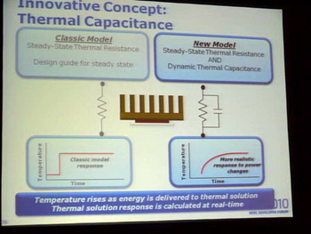 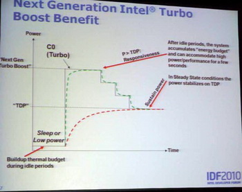   Four core processor from default 3,4 GHz can reach in peak load 4,9 GHz. We do not forget also about the presence of hyper threading technology 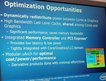 Related Products : | ||
|
|
||
|
xtreview is your : Video card - cpu - memory - Hard drive - power supply unit source |
|
|
|
|
||
|
Xtreview Support  N-Post:xxxx Xtreview Support  |
SANDY BRIDGE CACHE SYSTEM |
| Please Feel Free to write any Comment; Thanks  |
SLI-bridges Asus with RGB-backlight Aura (2017-05-12)
Asus unveiled new SLI-bridges to Pascal in style Strix cards (2017-01-17)
Sandy Bridge record SuperPI 32M at a frequency of 5948 MHz (2016-12-20)
Cheap SLI-bridges Pascal got to Japan (2016-12-17)
Asus offers a SLI-bridges to Pascal strict design (2016-12-15)
MSI SLI bridges for the new NVIDIA cards (2016-09-20)
What is special about the new SLI-bridge for Pascal (2016-08-12)
EVGA launches sales of Pascal SLI-bridge (2016-06-22)
Intel eof server processors Xeon E7 v2 Ivy Bridge-EX (2016-06-13)
MSI has shown a cooling system for processors and new SLI-bridges (2016-05-31)
TSMC will produce Silicon Bridge for NVIDIA GP100 Pascal (2016-04-04)
Ivy Bridge on a single core clocked up to 7189 MHz (2016-03-21)
MSI has decided to attach to the SLI-bridges fans (2016-03-20)
Ivy Bridge processor at a frequency of 7.07 GHz (2016-02-20)
UMC only now announced the launch of mass production of silicon bridges for AMD Fiji (2015-07-21)
MSI SLI-bridges reached stores (2015-07-20)
The manufacturing and packaging Bridge GPU Fiji and HBM memory (2015-06-18)
Intel says goodbye to Ivy Bridge-E processors (2015-06-04)
MSI is also preparing branded SLI-backlit bridges (2015-06-04)
AMD SkyBridge project was delayed due to GlobalFoundries (2015-05-17)
![]()

To figure out your best laptops .Welcome to XTreview.com. Here u can find a complete computer hardware guide and laptop rating .More than 500 reviews of modern PC to understand the basic architecture


7600gt review
7600gt is the middle card range.
We already benchmarked this video card and found that ...
 geforce 8800gtx and 8800gts Xtreview software download Section AMD TURION 64 X2 REVIEW INTEL PENTIUM D 920 , INTEL PENTIUM D 930 6800XT REVIEW computer hardware REVIEW INTEL CONROE CORE DUO 2 REVIEW VS AMD AM2 INTEL PENTIUM D 805 INTEL D805 Free desktop wallpaper online fighting game Xtreview price comparison center
Rss Feeds

- The new version of GPU-Z finally kills the belief in the miracle of Vega transformation
- The motherboard manufacturer confirms the characteristics of the processors Coffee Lake
- We are looking for copper coolers on NVIDIA Volta computing accelerators
- Unofficially about Intels plans to release 300-series chipset
- The Japanese representation of AMD offered monetary compensation to the first buyers of Ryzen Threadripper
- This year will not be released more than 45 million motherboards
- TSMC denies the presentation of charges from the antimonopoly authorities
- Radeon RX Vega 64 at frequencies 1802-1000 MHz updated the record GPUPI 1B
- AMD itself would like to believe that mobile processors Ryzen have already been released
- AMD Vega 20 will find application in accelerating computations
- Pre-orders for new iPhone start next week
- Radeon RX Vega 57, 58 and 59: the wonders of transformation
- ASML starts commercial delivery of EUV-scanners
- The older Skylake processors with a free multiplier are removed from production
- Meizu will release Android-smartphone based on Helio P40
- AMD Bristol Ridge processors are also available in American retail
- The fate of Toshiba Memory can be solved to the next environment
- duo GeForce GTX 1080 Ti in GPUPI 1B at frequencies of 2480-10320 MHz
- New Kentsfield overclocking record up to 5204 MHz
- Lenovo released Android-smartphone K8


computer news computer parts review Old Forum Downloads New Forum Login Join Articles terms Hardware blog Sitemap Get Freebies