OOPS! You forgot to upload swfobject.js ! You must upload this file for your form to work.
Toshiba has introduced 16-crystal stack memory using TSVs
![]()
|
xtreview is your : Video card - cpu - memory - Hard drive - power supply unit source |
|
|||
|
|
||||
 Recommended : Free unlimited image hosting with image editor
|
POSTER: computer news || TOSHIBA HAS INTRODUCED 16-CRYSTAL STACK MEMORY USING TSVS |
DATE:2015-08-07 |
|
|
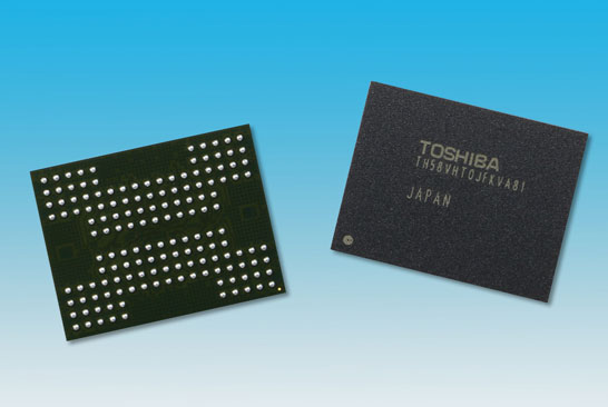
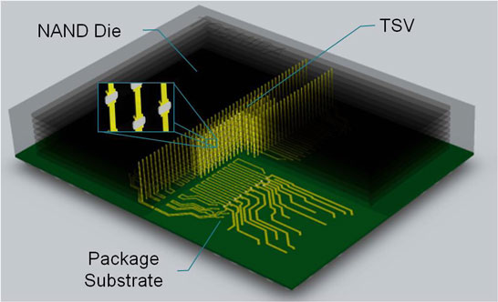
Multilayer flash memory NAND-type has 32-48 workers. All layers permeates through connection type TSVs. In fact - it is filled with metal channels conductors. But in case of 3D NAND memory cell channels are formed directly around the metallization. Simply put, TSVs - it is an integral part of the memory cells. Meanwhile, the type of connection used TSVs began long before the multi-layered memory. First practice for the assembly of multi-chip packaging method through channels metallization was by Samsung company . In 2007, the manufacturer introduced a multi-chip stack layout of the four 64-Mbyte crystals DDR2, collected by TSVs. Until this moment the stacks of crystals 20 pieces assembled by using the outer wire harnesses. This required considerable free space around the working of the crystal, as well as significantly increased operating currents as increasing the length of the connecting conductors.  Toshiba Company, as reported to us a press release , is not going to part with the multi-chip stack package using TSVs, even in light of the transition to a multi-layer 3D NAND. The Japanese manufacturer introduced the 8- and 16-crystal assembly gathered using TSVs-connections. In this case, channels TSVs - conductors is simply not participating in the organization of memory cells. However, this approach, as stated above, enables to minimize the area of each crystal in the grid and reduce the current load. According to Toshiba, the performance of the read / write memory consumption is reduced by 50%.  Demonstration development held on August 11 at the event, Flash Memory Summit 2015. The company has prepared two samples: 8-level 128-GB chip and 16-level 256 GB. The rate of exchange at the interface assembly may exceed 1 Gb / s. Stated interface - Toggle DDR.
Related Products : | ||
|
|
||
|
xtreview is your : Video card - cpu - memory - Hard drive - power supply unit source |
|
|
|
|
||
|
Xtreview Support  N-Post:xxxx Xtreview Support        |
TOSHIBA HAS INTRODUCED 16-CRYSTAL STACK MEMORY USING TSVS |
| Please Feel Free to write any Comment; Thanks  |
The six-core processor Intel Coffee Lake has conquered the frequency of 5.0 GHz (2017-09-05)
Micron has sold Lexar assets to Chinese (2017-09-05)
One more copy of Core i9-7960X has overcome a boundary of 5000 points in Cinebench R15 (2017-09-04)
Morningstar experts believe that Intel has a good potential in the field of artificial intelligence (2017-09-04)
Samsung has released an Android-smartphone Galaxy J7 plus with a dual camera (2017-09-04)
Over the past week, the Monero rate has almost doubled (2017-08-24)
The virtual reality helmet of HTC Vive has fallen in price to 599 per set (2017-08-22)
GlobalFoundries has become the worlds second largest manufacturer, which can produce solutions like AMD Vega (2017-08-17)
Over the past three months, NVIDIA has earned at least 150 million (2017-08-11)
Core i9-7900X at 5960 MHz has updated the GPUPI for CPU 1B (2017-08-08)
Tesla Model X has become cheaper (2017-08-05)
Steam has an independent version of Call of Duty Modern Warfare Remastered (2017-07-28)
Tesla has enlarged the options packages and is preparing to abolish the minor version of Model S (2017-07-24)
Core i9-7900X has updated the Cinebench R11.5 record at 5941 MHz (2017-07-22)
GeForce GTX 1080 Ti on the frequency of the chip 2632 MHz has updated the records 3DMark Fire Strike (2017-07-19)
Asus has finalized the cooling system of the ROG Rampage VI Apex board Intel X299 (2017-07-14)
Popularity of cryptocurrency as a means of payment has not grown (2017-07-13)
The manufacturer has nothing to do with the Pentium G4560 (2017-07-12)
Set of Oculus Rift and manipulators Oculus Touch has fallen in price to 399 dollars (2017-07-10)
Intel Pentium G4560 turned out so good that Intel has to reduce its sales (2017-07-10)
![]()
To figure out your best laptops .Welcome to XTreview.com. Here u can find a complete computer hardware guide and laptop rating .More than 500 reviews of modern PC to understand the basic architecture


7600gt review
7600gt is the middle card range.
We already benchmarked this video card and found that ...

 geforce 8800gtx and 8800gts
  Xtreview software download Section
  AMD TURION 64 X2 REVIEW
  INTEL PENTIUM D 920 , INTEL PENTIUM D 930
  6800XT REVIEW
  computer hardware REVIEW
  INTEL CONROE CORE DUO 2 REVIEW VS AMD AM2
  INTEL PENTIUM D 805 INTEL D805
  Free desktop wallpaper
  online fighting game
  Xtreview price comparison center
 Lastest 15 Reviews


Rss Feeds
Last News
- The new version of GPU-Z finally kills the belief in the miracle of Vega transformation
- The motherboard manufacturer confirms the characteristics of the processors Coffee Lake
- We are looking for copper coolers on NVIDIA Volta computing accelerators
- Unofficially about Intels plans to release 300-series chipset
- The Japanese representation of AMD offered monetary compensation to the first buyers of Ryzen Threadripper
- This year will not be released more than 45 million motherboards
- TSMC denies the presentation of charges from the antimonopoly authorities
- Radeon RX Vega 64 at frequencies 1802-1000 MHz updated the record GPUPI 1B
- AMD itself would like to believe that mobile processors Ryzen have already been released
- AMD Vega 20 will find application in accelerating computations
- Pre-orders for new iPhone start next week
- Radeon RX Vega 57, 58 and 59: the wonders of transformation
- ASML starts commercial delivery of EUV-scanners
- The older Skylake processors with a free multiplier are removed from production
- Meizu will release Android-smartphone based on Helio P40
- AMD Bristol Ridge processors are also available in American retail
- The fate of Toshiba Memory can be solved to the next environment
- duo GeForce GTX 1080 Ti in GPUPI 1B at frequencies of 2480-10320 MHz
- New Kentsfield overclocking record up to 5204 MHz
- Lenovo released Android-smartphone K8

HALO 3 HALO 3 - Final Fight!

PREY Prey is something you don t often see anymore: a totally unigue shooter experience.

computer news computer parts review Old Forum Downloads New Forum Login Join Articles terms Hardware blog Sitemap Get Freebies


