OOPS! You forgot to upload swfobject.js ! You must upload this file for your form to work.
Micron starts shipping engineering samples memory Hybrid Memory Cube
![]()
|
xtreview is your : Video card - cpu - memory - Hard drive - power supply unit source |
|
|||
|
|
||||
 Recommended : Free unlimited image hosting with image editor
|
POSTER: computer news || MICRON STARTS SHIPPING ENGINEERING SAMPLES MEMORY HYBRID MEMORY CUBE |
DATE:2013-09-27 |
|
|
In early September, a developer and manufacturer of programmable FPGA-matrix - Altera company - announced the release of kits for the evaluation of a new memory type in the face of Hybrid Memory Cube (HMC). At the same board were four high-performance SoC Altera and only one memory chip HMC from Micron production . The capacity of this memory at this stage is 160 Gb / s, allowing it to provide access to both the four processors no limit for each of them. In this case, the capacity of one chip HMC is 2 GB, which is equivalent to a single strip of memory. From now on, Micron company , engineering samples of the 2-GB memory HMC available to the public. In early 2014, the company expect to start production of engineering samples Hybrid Memory Cube 4GB. However, the company did not disclose details about the composition of these chips, as no data on the technical process, in which Micron manufactures HMC. Theoretically, a stack of memory chips and a controller may consist of 9 layers. 2 GB chip, as seen in the photo, made up of 5 layers, 4 of which - a 4-Gbit memory.  However, it remains unknown who released engineering samples Hybrid Memory Cube. Micron company , possibly at its factory such technology is not yet mastered. But its partner in the development of specifications HMC - Samsung company - can not only connect the crystals with through channels, but also produce real three-dimensional semiconductor structures. In other words, if HMC memory will get a strong demand, Samsung without any problems start producing such a memory. According to Micron estimates , serial production of Hybrid Memory Cube for commercial use will do not start at the end of 2014, then in 2015. At first, it will supply the specific needs related to the scope of FPGA use and specialized SoC. In the consumer electronics memory Hybrid Memory Cube will be no earlier than 3 years, and even after 5 years.  Memory Micron Hybrid Memory Cube - is a special case of the so-called broadband memory HBM (High Bandwidth Memory). There are several standard HBM, specifications developed by sectoral committee JEDEC.
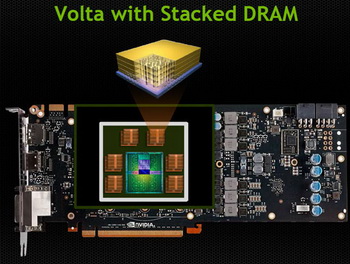
 In general, it is about expanding the bit interface circuits up to 1024 bits (standard Wide I / O), using cross-connections (TSVs) and moving the controller in the chip. This type of memory, for example, is going to be used in the architecture of NVIDIA Corporation in 2015 under the code name of Volta .  Related Products : | ||
|
|
||
|
xtreview is your : Video card - cpu - memory - Hard drive - power supply unit source |
|
|
|
|
||
|
Xtreview Support  N-Post:xxxx Xtreview Support        |
MICRON STARTS SHIPPING ENGINEERING SAMPLES MEMORY HYBRID MEMORY CUBE |
| Please Feel Free to write any Comment; Thanks  |
ASML starts commercial delivery of EUV-scanners (2017-09-07)
Open beta testing Star Wars Battlefront II starts in early October (2017-07-10)
The new season of Life is Strange starts at the end of summer (2017-06-12)
Western Digital Corporation starts mass production of 64-layer 3D NAND memory capacity increased (2017-02-07)
Japan Display starts production of improved 5-inch display with a resolution WQHD (2017-01-20)
Tesla Motors limits the number of sudden starts on a number of models (2016-12-26)
The cost of Android-smartphone Nokia D1C starts at 150 dollars (2016-12-12)
Samsung starts production of 10-nm processor Qualcomm Snapdragon 835 (2016-11-18)
HTC starts taking orders for the wireless connection kit for Vive (2016-11-12)
Samsung starts 10-nm products mass production (2016-10-17)
Intel 3D XPoint memory starts in the series Optane 8000p (2016-10-16)
Intel starts shipping 14-nm Stratix matrices 10 ARM Cortex-A53 architecture (2016-10-06)
EVGA starts to distribute L-shaped adapter to power the video card (2016-10-04)
Pre-orders for Core i7-7700K Kaby Lake already starts (2016-09-18)
Samsung starts shipping SSD-drives M.2 PCIe NVMe Samsung SM961 Series (2016-06-23)
Seagate starts massive supply 10-terabyte hard drives (2016-04-28)
HTC starts shipping virtual reality helmet Vive (2016-04-06)
Samsung starts production of DDR4 chips at 10-nm class technology (2016-04-05)
LG starts selling budget smartphone K5 and K8 (2016-03-15)
Samsung starts sales of laptops and tablets Notebook 9 Galaxy TabPro S (2016-03-06)
![]()
To figure out your best laptops .Welcome to XTreview.com. Here u can find a complete computer hardware guide and laptop rating .More than 500 reviews of modern PC to understand the basic architecture


7600gt review
7600gt is the middle card range.
We already benchmarked this video card and found that ...

 geforce 8800gtx and 8800gts
  Xtreview software download Section
  AMD TURION 64 X2 REVIEW
  INTEL PENTIUM D 920 , INTEL PENTIUM D 930
  6800XT REVIEW
  computer hardware REVIEW
  INTEL CONROE CORE DUO 2 REVIEW VS AMD AM2
  INTEL PENTIUM D 805 INTEL D805
  Free desktop wallpaper
  online fighting game
  Xtreview price comparison center
 Lastest 15 Reviews


Rss Feeds
Last News
- The new version of GPU-Z finally kills the belief in the miracle of Vega transformation
- The motherboard manufacturer confirms the characteristics of the processors Coffee Lake
- We are looking for copper coolers on NVIDIA Volta computing accelerators
- Unofficially about Intels plans to release 300-series chipset
- The Japanese representation of AMD offered monetary compensation to the first buyers of Ryzen Threadripper
- This year will not be released more than 45 million motherboards
- TSMC denies the presentation of charges from the antimonopoly authorities
- Radeon RX Vega 64 at frequencies 1802-1000 MHz updated the record GPUPI 1B
- AMD itself would like to believe that mobile processors Ryzen have already been released
- AMD Vega 20 will find application in accelerating computations
- Pre-orders for new iPhone start next week
- Radeon RX Vega 57, 58 and 59: the wonders of transformation
- ASML starts commercial delivery of EUV-scanners
- The older Skylake processors with a free multiplier are removed from production
- Meizu will release Android-smartphone based on Helio P40
- AMD Bristol Ridge processors are also available in American retail
- The fate of Toshiba Memory can be solved to the next environment
- duo GeForce GTX 1080 Ti in GPUPI 1B at frequencies of 2480-10320 MHz
- New Kentsfield overclocking record up to 5204 MHz
- Lenovo released Android-smartphone K8

HALO 3 HALO 3 - Final Fight!

PREY Prey is something you don t often see anymore: a totally unigue shooter experience.

computer news computer parts review Old Forum Downloads New Forum Login Join Articles terms Hardware blog Sitemap Get Freebies


