OOPS! You forgot to upload swfobject.js ! You must upload this file for your form to work.
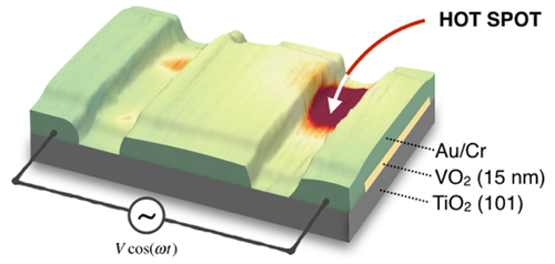
IBM made thermometer for quick search of overheating in the chips with the norms of less than 14 nm
![]()
|
xtreview is your : Video card - cpu - memory - Hard drive - power supply unit source |
|
|||
|
|
||||
 Recommended : Free unlimited image hosting with image editor
|
xtreview is your : Video card - cpu - memory - Hard drive - power supply unit source |
|
|
|
|
||
|
Xtreview Support  N-Post:xxxx Xtreview Support        |
IBM MADE THERMOMETER FOR QUICK SEARCH OF OVERHEATING IN THE CHIPS WITH THE NORMS OF LESS THAN 14 NM |
| Please Feel Free to write any Comment; Thanks  |
The decision on the transaction between WDC and Toshiba can be made on August 31 (2017-08-27)
Reviews Intel Core i9-7900X will be made public on Monday (2017-06-16)
Ready-made systems based on AMD Ryzen Threadripper will be released in late July (2017-06-14)
Power Supply Cooler Master MasterWatt Maker 1200 MIJ 1.2 kW, made in Japan and only 999 euros (2017-03-09)
IBM made thermometer for quick search of overheating in the chips with the norms of less than 14 nm (2016-12-06)
The number of customers in the direction of AMD custom-made products will increase (2016-10-21)
GeForce GTX 1070 made 20 000 points in 3DMark Fire Strike (2016-10-09)
Enthusiast made quality crystal photo of GPU NVIDIA GP104 (2016-09-20)
Samsung has made an official statement about the exploding Galaxy Note 7 (2016-09-02)
Jonsbo VR2 is made of steel, aluminum and glass (2016-08-02)
Scientists have made graphene in a light bulb (2016-06-19)
Roomy case Anidees AI Crystal is made of steel and tempered glass (2016-06-13)
The side panel of In Win 303 is made of tempered glass (2016-05-19)
Phanteks Enthoo Evolv ATX Tempered Glass Edition made of glass (2016-04-30)
SoC platform MediaTek Helio X30 will be made on 10-nm process technology (2016-04-27)
AMD managed to get three new customers in the custom-made solutions (2016-04-22)
Side Jonsbo C3 Window wall made of tempered glass (2016-04-12)
Power Supplies Lian Li PE-750 and PE-550 are made in the form factor SFX-L (2016-04-11)
Power Supply Corsair SF600 and SF450 are made in the form factor SFX (2016-03-09)
AnTuTu made a rating of the ten most productive single-chip platforms (2016-03-07)
![]()
To figure out your best laptops .Welcome to XTreview.com. Here u can find a complete computer hardware guide and laptop rating .More than 500 reviews of modern PC to understand the basic architecture


7600gt review
7600gt is the middle card range.
We already benchmarked this video card and found that ...

 geforce 8800gtx and 8800gts
  Xtreview software download Section
  AMD TURION 64 X2 REVIEW
  INTEL PENTIUM D 920 , INTEL PENTIUM D 930
  6800XT REVIEW
  computer hardware REVIEW
  INTEL CONROE CORE DUO 2 REVIEW VS AMD AM2
  INTEL PENTIUM D 805 INTEL D805
  Free desktop wallpaper
  online fighting game
  Xtreview price comparison center
 Lastest 15 Reviews


Rss Feeds
Last News
- The new version of GPU-Z finally kills the belief in the miracle of Vega transformation
- The motherboard manufacturer confirms the characteristics of the processors Coffee Lake
- We are looking for copper coolers on NVIDIA Volta computing accelerators
- Unofficially about Intels plans to release 300-series chipset
- The Japanese representation of AMD offered monetary compensation to the first buyers of Ryzen Threadripper
- This year will not be released more than 45 million motherboards
- TSMC denies the presentation of charges from the antimonopoly authorities
- Radeon RX Vega 64 at frequencies 1802-1000 MHz updated the record GPUPI 1B
- AMD itself would like to believe that mobile processors Ryzen have already been released
- AMD Vega 20 will find application in accelerating computations
- Pre-orders for new iPhone start next week
- Radeon RX Vega 57, 58 and 59: the wonders of transformation
- ASML starts commercial delivery of EUV-scanners
- The older Skylake processors with a free multiplier are removed from production
- Meizu will release Android-smartphone based on Helio P40
- AMD Bristol Ridge processors are also available in American retail
- The fate of Toshiba Memory can be solved to the next environment
- duo GeForce GTX 1080 Ti in GPUPI 1B at frequencies of 2480-10320 MHz
- New Kentsfield overclocking record up to 5204 MHz
- Lenovo released Android-smartphone K8

HALO 3 HALO 3 - Final Fight!

PREY Prey is something you don t often see anymore: a totally unigue shooter experience.

computer news computer parts review Old Forum Downloads New Forum Login Join Articles terms Hardware blog Sitemap Get Freebies


